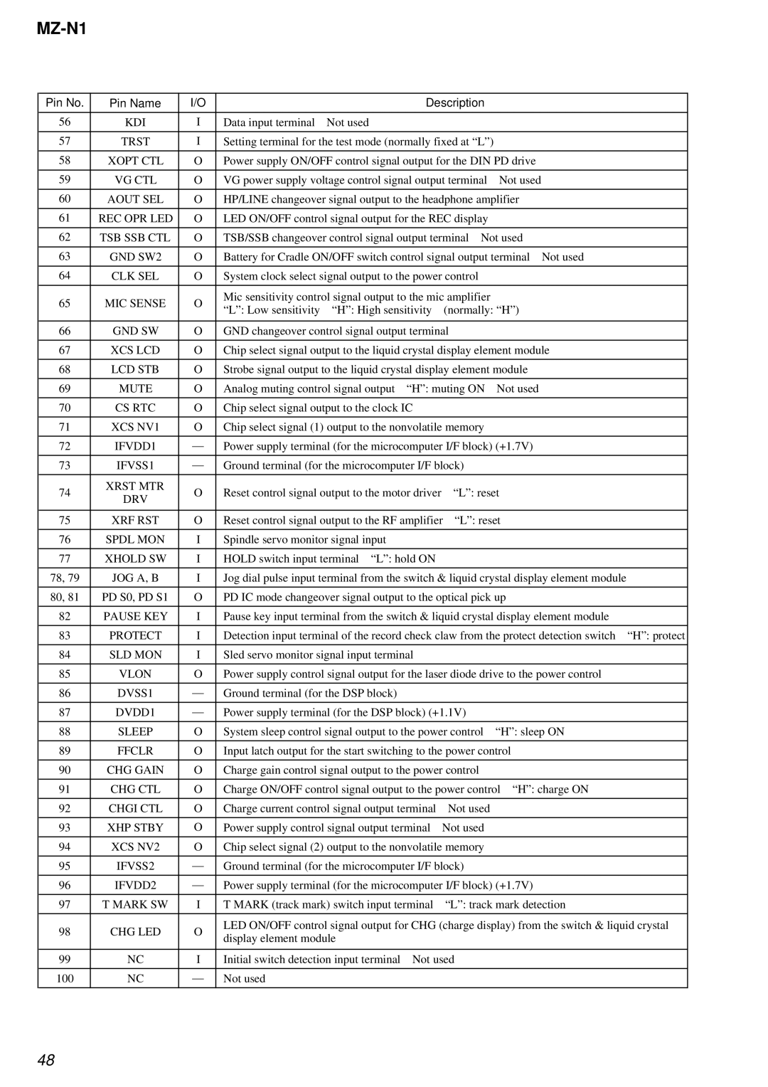
MZ-N1 specifications
The Sony MZ-N1, a revered model in the world of portable mini-disc players, holds a special place in the hearts of audiophiles and casual listeners alike. Launched as part of Sony's celebrated mini-disc lineup, it exemplifies the innovative spirit of its time with a sleek, compact design and a suite of features that appealed to music lovers.At the heart of the MZ-N1 is its support for both standard and high-speed recording, allowing users to transfer their favorite tracks from CDs or other sources quickly and efficiently. The unit employs a unique mechanism known as the ATRAC codec, which optimizes audio compression while maintaining sound quality. This technology enables users to fit numerous tracks onto a single mini-disc, transforming how music was stored and played back.
One of its standout features is the inclusion of SonicStage software, which serves as a companion for managing music libraries. Users can edit playlists, transfer tracks, and organize their music collection seamlessly. The player supports various formats, including MP3, making it versatile in its playback capabilities. Additionally, the MZ-N1 is equipped with a backlit display, facilitating easy navigation even in low-light conditions.
Another notable characteristic of the MZ-N1 is its impressive battery life, offering hours of continuous playback on a single charge. This longevity made it an attractive option for users on the go, ensuring that their music would last through long commutes or road trips without interruption.
Furthermore, the MZ-N1 features a headphone amplifier that enhances sound quality, providing a richer audio experience. The player boasts a range of sound customizations, allowing users to adjust equalizer settings to suit their preferred listening style.
In terms of design, the MZ-N1 is compact, lightweight, and sturdy, making it highly portable. The simple, intuitive interface ensures that users can navigate through functions with ease, enhancing the overall listening experience.
Overall, the Sony MZ-N1 stands as a remarkable blend of technology and user-friendly design, showcasing the innovation of the early 2000s portable audio solutions. Its combination of sound quality, flexibility, and battery efficiency has solidified its status as a classic in the realm of mini-disc players. While modern digital music players have largely eclipsed this technology, the legacy of the MZ-N1 endures in the memories of those who experienced its audio marvels.
