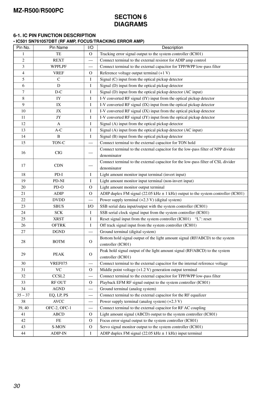
R500PC specifications
The Sony R500PC is a notable addition to the line of personal computers designed to cater to the needs of both professionals and casual users alike. This all-in-one desktop computer combines advanced technology with a sleek, modern design, making it an attractive choice for various applications ranging from office work to multimedia entertainment.One of the standout features of the Sony R500PC is its powerful processor. Equipped with the latest generation Intel Core i5 or i7 chip, the R500PC delivers exceptional performance that can handle multitasking with ease. Users can run multiple programs simultaneously without experiencing any lag, making it ideal for professionals who require efficiency in their daily tasks.
The R500PC boasts a high-definition display, featuring a resolution of 1920x1080 pixels. This Full HD screen offers vibrant colors and sharp details, enhancing the viewing experience for gaming, movies, and graphic design work. The display is also touch-enabled, providing an intuitive user interface that allows for seamless navigation through applications, web browsing, and photo editing.
Another key characteristic of the Sony R500PC is its extensive storage options. It typically comes with a solid-state drive (SSD) or a hybrid drive configuration, ensuring quick boot times and faster file access. With storage capacities ranging from 256GB to 1TB, users have ample space to store their documents, media files, and applications without worrying about running out of space.
In terms of connectivity, the Sony R500PC offers a robust set of ports including USB 3.0, HDMI, and Ethernet, providing flexibility in connecting external devices such as printers, external hard drives, and displays. Additionally, it features built-in Wi-Fi and Bluetooth capabilities, facilitating wireless communication and data transfer.
The audio system on the R500PC is another highlight. With integrated speakers that deliver clear and loud sound, users can enjoy a rich audio experience during video playback and gaming sessions. The device also supports high-definition audio output for a more immersive experience.
Lastly, the Sony R500PC is designed with energy efficiency in mind. It comes with power-saving features and has received environmental certifications, making it a sustainable choice for environmentally-conscious consumers.
In conclusion, the Sony R500PC is a feature-packed personal computer that excels in performance, display quality, storage options, and connectivity. Whether for work or leisure, this all-in-one PC is set to deliver a versatile computing experience that meets the demands of modern users. With its stylish design and robust capabilities, the R500PC stands out as an excellent investment for anyone looking to upgrade their technology.
