• Semiconductor Location (MAIN BOARD)
Ref. No. | Location |
| Ref. No. | Location |
D104 |
| Q103 | ||
D106 |
| Q104 | ||
D107 |
| Q105 | ||
D108 |
| Q106 | ||
D109 |
| Q107 | ||
D204 |
| Q108 | ||
D206 |
| Q109 | ||
D207 |
| Q110 | ||
D208 |
| Q111 | ||
D209 |
| Q112 | ||
D701 |
| Q113 | ||
D702 |
| Q114 | ||
D703 |
| Q201 | ||
D801 |
| Q202 | ||
D802 |
| Q203 | ||
D803 |
| Q204 | ||
D820 |
| Q205 | ||
D822 |
| Q206 | ||
D827 |
| Q207 | ||
D832 |
| Q208 | ||
D850 |
| Q209 | ||
D851 |
| Q210 | ||
D852 |
| Q211 | ||
D853 |
| Q212 | ||
D854 |
| Q213 | ||
D901 |
| Q214 | ||
D902 |
| Q701 | ||
D905 |
| Q702 | ||
D906 |
| Q801 | ||
D909 |
| Q802 | ||
D910 |
| Q803 | ||
D911 |
| Q804 | ||
D912 |
| Q805 | ||
D913 |
| Q806 | ||
D914 |
| Q809 | ||
D915 |
| Q901 | ||
D917 |
| Q902 | ||
D918 |
| Q903 | ||
D919 |
| Q904 | ||
D920 |
| Q905 | ||
|
|
| Q906 | |
IC101 |
| Q907 | ||
IC102 |
| Q908 | ||
IC202 |
| Q909 | ||
IC301 |
| Q910 | ||
IC302 |
| Q911 | ||
IC901 |
| Q912 | ||
IC902 |
| Q913 | ||
IC903 |
| Q914 | ||
|
|
| Q915 | |
Q101 |
| Q920 | ||
Q102 |
|
|
| |
|
|
|
|
|
XM-SD22X
THIS NOTE IS COMMON FOR PRINTED WIRING BOARDS AND SCHEMATIC DIAGRAMS.
(In addition to this, the necessary note is printed in each block.)
for schematic diagram: Note:
•All capacitors are in ∝F unless otherwise noted. (p: pF) 50 WV or less are not indicated except for electrolytics and tantalums.
•All resistors are in Ω and 1/4 W or less unless otherwise specified.
•% : indicates tolerance.
•2 : nonflammable resistor.
•C : panel designation.
Note: | Note: |
The components identi- | Les composants identifiés par |
fied by mark 0 or dotted | une marque 0 sont critiques |
line with mark 0 are criti- | pour la sécurité. |
cal for safety. | Ne les remplacer que par une |
Replace only with part | piéce portant le numéro |
number specified. | spécifié. |
|
|
•A : B+ Line.
•B : B– Line.
•H : adjustment for repair.
•Power voltage is dc 14.4V and fed with regulated dc power supply from +12V and REM terminals.
•Voltage and waveform are dc with respect to ground under
•Voltages are taken with a VOM (Input impedance 10 MΩ). Voltage variations may be noted due to normal produc- tion tolerances.
•Waveforms are taken with a oscilloscope.
Voltage variations may be noted due to normal produc- tion tolerances.
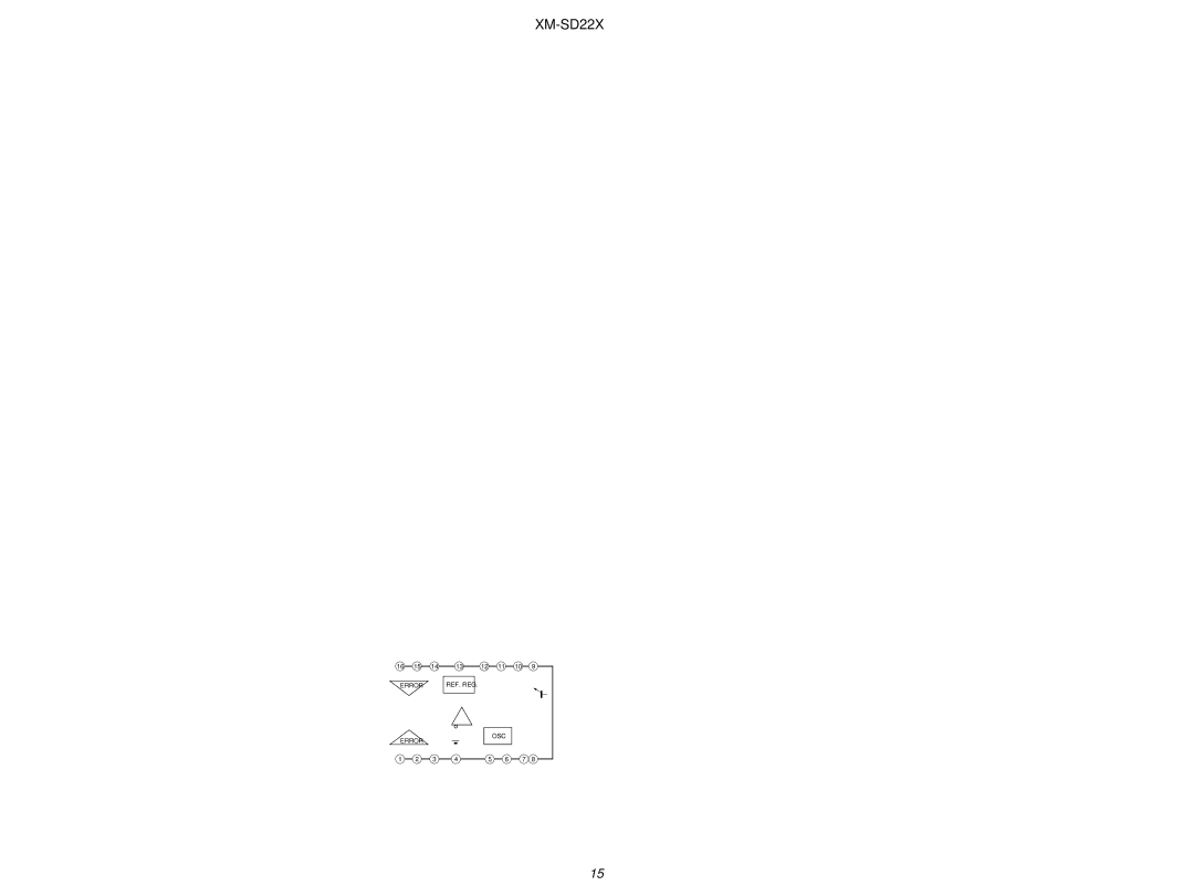
•Circled numbers refer to waveforms.
•Signal path.
F : AUDIO
for printed wiring boards: Note:
•X : parts extracted from the component side.
•![]() : Pattern from the side which enables seeing.
: Pattern from the side which enables seeing.
• Waveform
1 IC901 5 |
15 ∝sec |
1V/div, 5 ∝sec/div |
15