
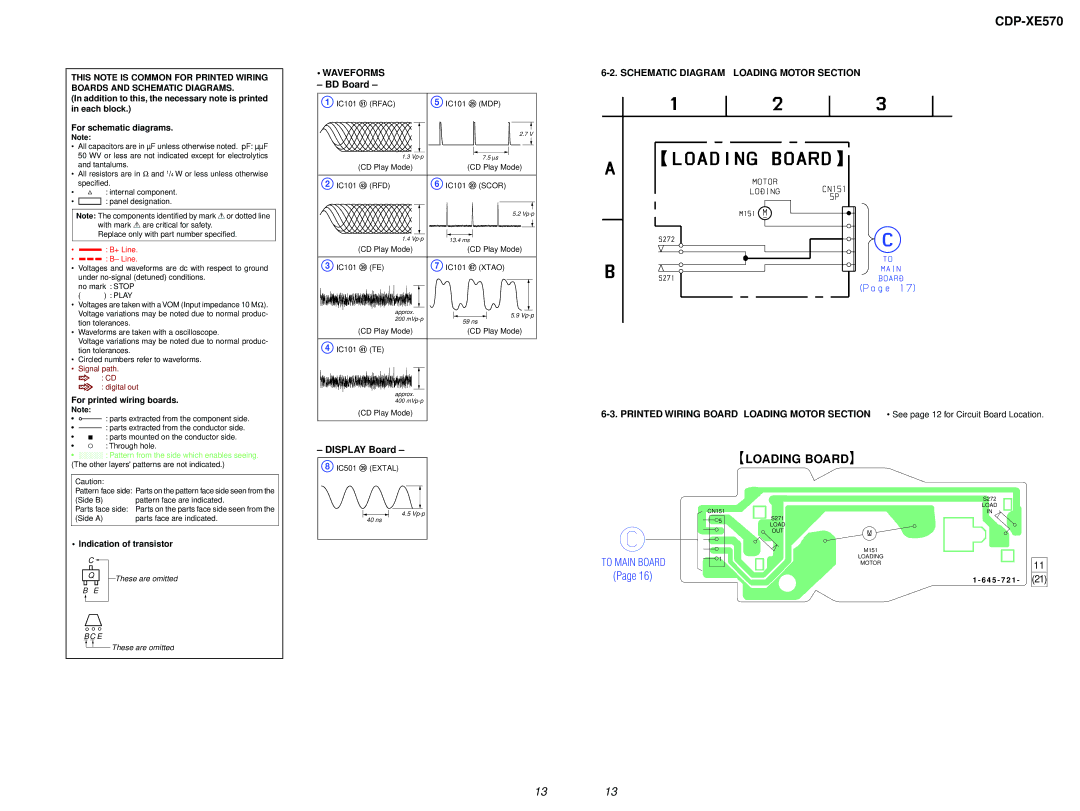
CDP-XE570 specifications
The Sony Ericsson CDP-XE570 is a significant entry in the realm of compact disc players, demonstrating the brand's commitment to audio fidelity and user-friendly design. Launched in the late 1990s, the CDP-XE570 became known for its impressive sound quality, making it a popular choice among audiophiles and casual listeners alike.One of the standout features of the CDP-XE570 is its precision-engineered digital-to-analog converter (DAC). This technology ensures that the audio playback is crisp, clear, and faithful to the original recording. The player supports various disc formats, including standard CDs, CD-R, and CD-RW, providing users with flexibility in their music choices. The presence of a high-quality laser pickup helps to minimize errors in playback, even for discs that may be scratched or smudged, enhancing the listening experience.
In terms of design, the CDP-XE570 boasts a sleek and compact form factor, allowing it to fit seamlessly into any home audio setup. Its straightforward control interface makes navigation easy, with well-placed buttons for play, pause, skip, and stop functions. The LCD display is clear and informative, providing readouts for track numbers and remaining playtime, which assists users in managing their music.
Another noteworthy characteristic of the CDP-XE570 is its compatibility with a variety of audio output options. The player includes both analog and digital outputs, allowing users to connect it to a range of audio systems, from vintage receivers to modern digital sound processors. This versatility ensures that the player can deliver high-quality sound whether paired with simple stereo systems or complex home theater setups.
Additionally, the CDP-XE570 incorporates advanced features like programmed playback and shuffle options, enabling users to customize their listening experience. A timer function is also included, which allows the player to schedule automatic playback, adding convenience for users who want to enjoy their favorite music at specific times.
Overall, the Sony Ericsson CDP-XE570 is more than just a compact disc player; it represents a blend of innovative technology and user-centric design. Its combination of high-quality audio playback, versatile connectivity options, and intuitive controls makes it a standout choice for anyone looking to enhance their music listening experience. With its reliable performance, the CDP-XE570 continues to hold a special place in the hearts of audio enthusiasts.