Safety Information and Technical Specifi cations
2-3 Front Jumper Locations and Pin Defi nitions
A | A | A | A | A | A | A | A |
C | C | C | C | C | C | C | C |
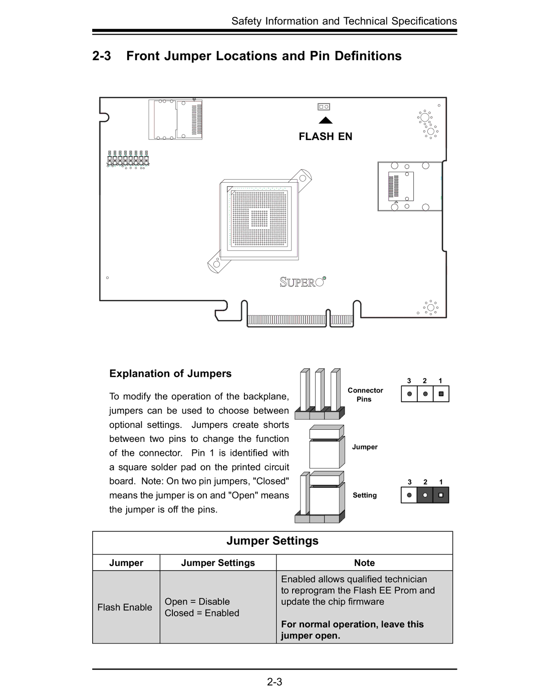
FLASH EN
1 | 2 | 3 | 4 | 5 | 6 | 7 | 8 | 9 | 10 | 12 | 14 | 16 | 18 | 20 | 22 | 24 | 26 |
|
|
|
|
|
|
|
|
| 11 | 13 | 15 | 17 | 19 | 21 |
| 23 | 25 |
A |
|
|
|
|
|
|
|
|
|
|
|
|
|
|
|
|
|
B |
|
|
|
|
|
|
|
|
|
|
|
|
|
|
|
|
|
C |
|
|
|
|
|
|
|
|
|
|
|
|
|
|
|
|
|
D |
|
|
|
|
|
|
|
|
|
|
|
|
|
|
|
|
|
E |
|
|
|
|
|
|
|
|
|
|
|
|
|
|
|
|
|
F |
|
|
|
|
|
|
|
|
|
|
|
|
|
|
|
|
|
G |
|
|
|
|
|
|
|
|
|
|
|
|
|
|
|
|
|
H |
|
|
|
|
|
|
|
|
|
|
|
|
|
|
|
|
|
J |
|
|
|
|
|
|
|
|
|
|
|
|
|
|
|
|
|
K |
|
|
|
|
|
|
|
|
|
|
|
|
|
|
|
|
|
L |
|
|
|
|
|
|
|
|
|
|
|
|
|
|
|
|
|
M |
|
|
|
|
|
|
|
|
|
|
|
|
|
|
|
|
|
N |
|
|
|
|
|
|
|
|
|
|
|
|
|
|
|
|
|
P |
|
|
|
|
|
|
|
|
|
|
|
|
|
|
|
|
|
R |
|
|
|
|
|
|
|
|
|
|
|
|
|
|
|
|
|
T |
|
|
|
|
|
|
|
|
|
|
|
|
|
|
|
|
|
U |
|
|
|
|
|
|
|
|
|
|
|
|
|
|
|
|
|
V |
|
|
|
|
|
|
|
|
|
|
|
|
|
|
|
|
|
W |
|
|
|
|
|
|
|
|
|
|
|
|
|
|
|
|
|
Y |
|
|
|
|
|
|
|
|
|
|
|
|
|
|
|
|
|
AA |
|
|
|
|
|
|
|
|
|
|
|
|
|
|
|
|
|
AB |
|
|
|
|
|
|
|
|
|
|
|
|
|
|
|
|
|
AC |
|
|
|
|
|
|
|
|
|
|
|
|
|
|
|
|
|
AD |
|
|
|
|
|
|
|
|
|
|
|
|
|
|
|
|
|
AE |
|
|
|
|
|
|
|
|
|
|
|
|
|
|
|
|
|
AF |
|
|
|
|
|
|
|
|
|
|
|
|
|
|
|
|
|
PCB EDGE |
PCB EDGE |
Explanation of Jumpers
To modify the operation of the backplane, jumpers can be used to choose between ![]()
![]()
![]()
![]() optional settings. Jumpers create shorts
optional settings. Jumpers create shorts ![]() between two pins to change the function
between two pins to change the function ![]() of the connector. Pin 1 is identified with
of the connector. Pin 1 is identified with
a square solder pad on the printed circuit
board. Note: On two pin jumpers, "Closed" means the jumper is on and "Open" means
the jumper is off the pins.
3 2 1
Connector
Pins
Jumper
3 2 1
Setting
Jumper Settings
Jumper | Jumper Settings | Note |
|
|
|
|
| Enabled allows qualified technician |
|
| to reprogram the Flash EE Prom and |
Flash Enable | Open = Disable | update the chip fi rmware |
| Closed = Enabled |
|
|
| For normal operation, leave this |
|
| jumper open. |
|
|
|
