Hardware Configuration
3.2.3Programming Interfaces (J30, J31)
The SPI of the device is used for writing to the control register of the device. It consists of three control lines CTRL_CLK, CTRL_DATA, and CTRL_LE. There are four
-Connect the parallel port cable to the PC and EVM parallel port. This needs control S/W (see Chapter 4).
3.2.4Loop Filter (J32−J34)
The loop filter is one of the key elements determining the loop bandwidth of the PLL. The loop filter converts the charge pump current into the control voltage for the voltage controlled oscillator. The phase difference between the input clocks of the phase frequency detector determines the width of the charge pump output current pulses. These high frequency pulses are transformed into a voltage to control the oscillator.
Basically, three types of loop filters are implemented on the EVM.
-Passive loop filter
-External active loop filter using an external
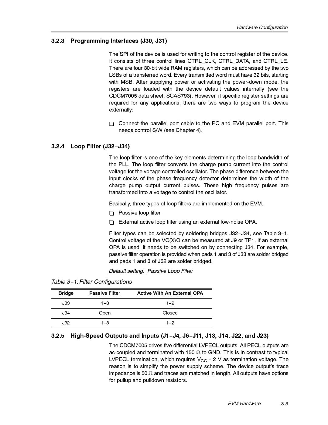
Filter types can be selected by soldering bridges J32−J34, see Table 3−1. Control voltage of the VC(X)O can be measured at J9 or TP1. If an external OPA is used, it needs to be switched on by connecting J34. For example, passive filter operation is provided when pads 1 and 3 of J33 are solder bridged and pads 1 and 3 of J32 are solder bridged.
Default setting: Passive Loop Filter
Table 3−1. Filter Configurations
Bridge | Passive Filter | Active With An External OPA |
|
|
|
J33 | 1−3 | 1−2 |
|
|
|
J34 | Open | Closed |
|
|
|
J32 | 1−3 | 1−2 |
|
|
|
3.2.5
The CDCM7005 drives five differential LVPECL outputs. All PECL outputs are
EVM Hardware |