TPA005D12 specifications
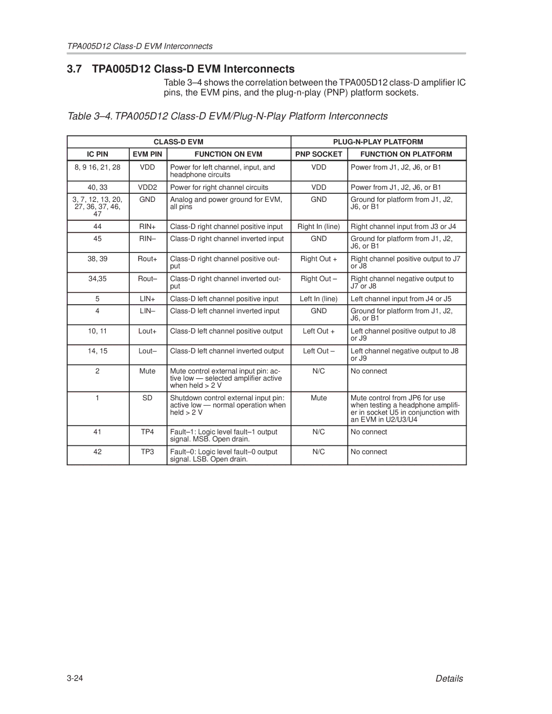
The Texas Instruments TPA005D12 is a highly regarded digital audio power amplifier that is engineered for high-performance applications. It is part of TI's TPA series, which is known for its efficient power delivery and superior sound quality. The TPA005D12 is designed to drive passive speakers while ensuring minimal power loss and efficient heat management.One of the standout features of the TPA005D12 is its ability to provide 5 watts of continuous output power per channel into an 8-ohm load with a low total harmonic distortion (THD) rating. This makes it suitable for use in a variety of audio applications, including computer speakers, soundbars, and portable audio systems. The amplifier operates from a single supply voltage, ranging typically from 4.5V to 14V, allowing for flexible integration into different power supply environments.
The TPA005D12 adopts Class-D amplification technology, which significantly enhances power efficiency compared to traditional linear amplifiers. Class-D amplifiers convert the input audio signal into a series of pulse-width modulated signals, resulting in increased power savings and reduced heat generation. This not only improves the overall energy efficiency but also contributes to a longer operational lifespan for devices utilizing this technology.
Additionally, the TPA005D12 features an integrated thermal and short-circuit protection mechanism, which helps safeguard the amplifier from potential damage due to excessive temperatures or electrical faults. This reliability factor is crucial for manufacturers looking to create robust consumer electronics.
Another important characteristic is its integrated low-noise power supply rejection ratio (PSRR), which helps maintain sound clarity and reduces the impact of power supply noise on audio quality. The TPA005D12 also supports differential input signals, which can improve common-mode noise rejection and further enhance audio performance.
The device is offered in a compact package suitable for space-constrained applications, enabling easy integration into various designs. With a combination of low cost, high efficiency, and excellent audio performance, the Texas Instruments TPA005D12 stands out as a top choice for developers and engineers seeking reliable audio amplification solutions. Whether in home entertainment systems or personal audio devices, the TPA005D12 is designed to deliver exceptional sound quality with a minimal footprint.

