TPS53125EVM-599 Assembly Drawings and Layout

www.ti.com

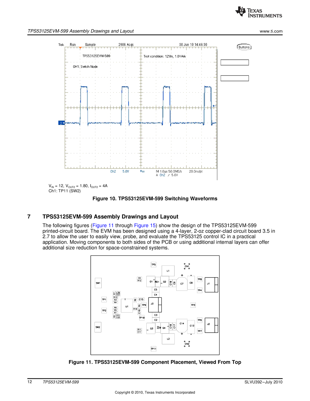
VIN = 12, VOUT2 = 1.80, IOUT2 = 4A

Ch1: TP11 (SW2)

Figure 10. TPS53125EVM-599 Switching Waveforms

7TPS53125EVM-599 Assembly Drawings and Layout

The following figures (Figure 11 through Figure 15) show the design of the TPS53125EVM-599 printed-circuit board. The EVM has been designed using a 4-layer, 2-oz copper-clad circuit board 3.5 in 2.7 to allow the user to easily view, probe, and evaluate the TPS53125 control IC in a practical application. Moving components to both sides of the PCB or using additional internal layers can offer additional size reduction for space-constrained systems.

Figure 11. TPS53125EVM-599 Component Placement, Viewed From Top

12

TPS53125EVM-599

SLVU392 –July 2010

Copyright © 2010, Texas Instruments Incorporated

Page 12
Image 12
Texas Instruments TPS53125EVM-599 Assembly Drawings and Layout, TPS53125EVM-599 Component Placement, Viewed From Top