GD-1220/1221
Page
Transportation/Installation
Vorsicht
Important Service Parts for Safety
Contents
2006 2008 Toshiba TEC Corporation All rights reserved
GD-1220 GD-1221 Remarks
FAX Options
STUDIO165/205 Available STUDIO167/207/237
System firmware version
Specifications
Transmission system
DBm to -8 dBm The setting can be changed by 1 dB
Embedded
DBm to 0 dBm Level -55 dBm or lower cannot be detected
Comp
Dimension width x length Printing area
Folio
Features
Specifications and Outline of System
08/08
Accessory Qty
Accessories and Parts
Following accessories and parts come with the FAX unit
Option Function Model
Extends the FAX functions when the FAX unit is installed
Options
ADF Radf
System List
NA/EU/AU/TW
Units and Components
Layout of PC Boards
Symbol Name Function
FAX
PWA-F-NCU-631
Recording paper size
LSU-RELATED Functions
Size Horizontal x Vertical Effective recording area
Effective recording area
Inch Feed direction Mm 0.16 inch Effective recording area
For MJD, AUD, ASD, SAD, TWD, and CND models Unit mm inch
Size Horizontal x Vertical Effective recording range
297 x 293 x A4-R 210 x 206 x A5-R 148 x 144 x 257 x 253 x
Print mode
Print algorithm
Recording paper selection algorithm and print algorithm
Recording paper selection algorithm
Judgment parameter
Reception print flowchart Start Receive FAX
Bit Discard parameter
Discard printing
Vertical reduction print
Similar reduction print
RTI
Scanning
For MJD, AUD, ASD, SAD, TWD, CND models
ST-R Comp
Scanning width
Recording paper range A4-R
For MJD, AUD, ASD, SAD, TWD, and CND models
Recording paper range
Comp *2 Comp *1
Recording paper range LT long Comp long LD long
Recording paper range A4 long B4 long A3 long
Folio Folio *1
Error processing
Order Drawer
Limitations on reception print
LSU-RELATED Functions
Dial call-up transmission to a telephone circuit
Circuit Connection and Procedure to Change Mode
YES
Standby state
Procedure to select the transmission mode
Selection of the communication mode
Communication mode Toshiba original procedure
Telephone circuit
Circuit control signals
Signaling System Diagram and Signal Forms
This signal can be sent manually Signal form
Signal name Signal form
Image signal
Communication with the binary signals
Mode change is possible only for the original set manually
Receiver
Frames received Error occurred
Only error frame retransmitted 1 completed 2 completed
MCF
CED Nsfcsidis
CFR
Binary signals
PIN
PIP
PRI-EOM
PRI-MPS
Format
When this frame is the last frame, X =
FCF FIF FCS
Binary signal Format
FCF format of each binary signal
TCF
9600 bps, 7200 bps
4800 bps, 2400 bps
3 V.8/V.34 communication sequence
Line closed
Standard procedure Transmitter Receiver
Signal name Abbreviation Function Remarks
Hz and 3,750 Hz in units
Tone signal between
150 Hz
Frequency transmission Capability
ALT
TRN
Receives an NSF sent from
Maintains the synchroniza 7E H Tion
Transmitter
Receiver
Scrambled data frame to be
Image data Image data are sent. Transmitter
Is completed
Encoded image data Turn off Scrambled 1 is sent for
PPS-EOP
Short training Signal
Transmission of one Is completed
Informs to disconnect the line
Line closed DIS cannot be recognized
DIALING/COMMUNICATION Control
DIALING/COMMUNICATION Control
DIALING/COMMUNICATION Control
DIALING/COMMUNICATION Control
TEL mode
FAX Automatic Switching
FAX mode
General functions
DIALING/COMMUNICATION Control
GD-1220/1221
Configuration
Description of Circuits
Configuration
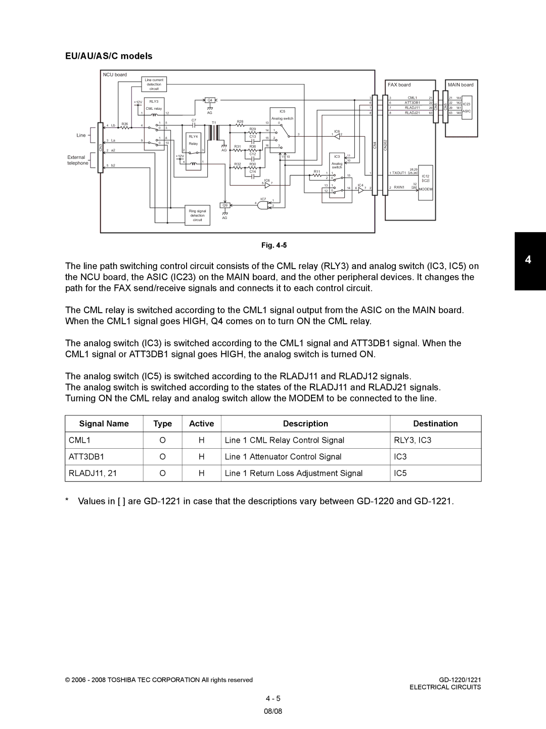
EU/AU/AS/C models
Signal Name Type Active Description Destination
Line path switching control circuit
CML1
ATT3DB1
IC5
RLY3, IC3
IC3
Dial pulse generation circuit
Line 1 Dial Pulse Generation Signal Q53
Line 1 Dial Pulse Generation Signal
Line Reverse Current Detection Signal IC23
Line Current Detection Signal IC23
Line current detection circuit
REVA1
Current Reverse Line 1 Current Detection IC23 Signal
Line 1 Current Detection Signal IC23
CI detection circuit
Line 1 CI Detect Signal IC23
Line 1 CI Detection Signal IC23
FAX board
Line monitor circuit
Ringer/Alarm
Monitoring signal
Line Monitor
LOW High
Sound volume
PWA-F-FAX-635 GD-1220
PC Boards
PWA-F-FAX-678 GD-1221 PWA-F-NCU-631 NAD, TWD, SAD
PWA-F-NCU-631 MJD, AUD, ASD, CND
Electrical Circuits
Explanation to the Users
Installation
Installation