TS1G~32GCF133 | 133X CompactFlash Card |
Feature Register (Address - 1F1h[171h]; Offset 1, 0Dh Write Only)
This register provides information regarding features of the CompactFlash Storage Card that the host can utilize. This register is also accessed in PC Card modes on data bits
Sector Count Register (Address - 1F2h[172h]; Offset 2)
This register contains the numbers of sectors of data requested to be transferred on a read or write operation between the host and the CompactFlash Storage Card. If the value in this register is zero, a count of 256 sectors is specified. If the command was successful, this register is zero at command completion. If not successfully completed, the register contains the number of sectors that need to be transferred in order to complete the request.
Sector Number (LBA 7-0) Register (Address - 1F3h[173h]; Offset 3)
This register contains the starting sector number or bits
6.1.5.5 Cylinder Low (LBA 15-8) Register (Address - 1F4h[174h]; Offset 4)
This register contains the low order 8 bits of the starting cylinder address or bits
Cylinder High (LBA 23-16) Register (Address - 1F5h[175h]; Offset 5)
This register contains the high order bits of the starting cylinder address or bits
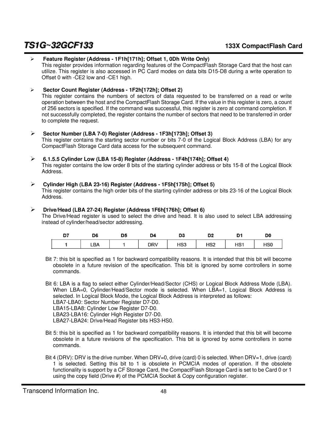
Drive/Head (LBA 27-24) Register (Address 1F6h[176h]; Offset 6)
The Drive/Head register is used to select the drive and head. It is also used to select LBA addressing instead of cylinder/head/sector addressing.
Bit 7: this bit is specified as 1 for backward compatibility reasons. It is intended that this bit will become obsolete in a future revision of the specification. This bit is ignored by some controllers in some commands.
Bit 6: LBA is a flag to select either Cylinder/Head/Sector (CHS) or Logical Block Address Mode (LBA). When LBA=0, Cylinder/Head/Sector mode is selected. When LBA=1, Logical Block Address is selected. In Logical Block Mode, the Logical Block Address is interpreted as follows:
Bit 5: this bit is specified as 1 for backward compatibility reasons. It is intended that this bit will become obsolete in a future revisions of the specification. This bit is ignored by some controllers in some commands.
Bit 4 (DRV): DRV is the drive number. When DRV=0, drive (card) 0 is selected. When DRV=1, drive (card) 1 is selected. Setting this bit to 1 is obsolete in PCMCIA modes of operation. If the obsolete functionality is support by a CF Storage Card, the CompactFlash Storage Card is set to be Card 0 or 1 using the copy field (Drive #) of the PCMCIA Socket & Copy configuration register.
Transcend Information Inc. | 48 |