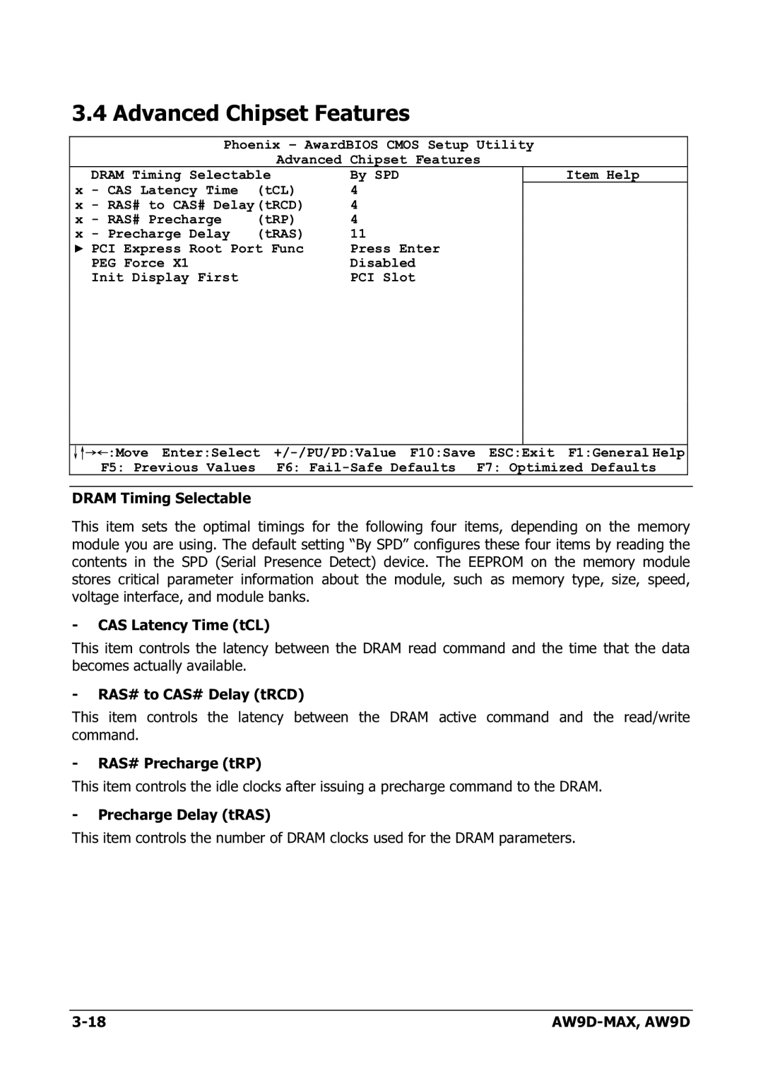
3.4 Advanced Chipset Features
Phoenix – AwardBIOS CMOS Setup Utility
Advanced Chipset Features
DRAM Timing | Selectable | By SPD | Item Help | |
x - CAS Latency Time | (tCL) | 4 |
| |
x - RAS# to CAS# Delay(tRCD) | 4 |
| ||
x - RAS# Precharge | (tRP) | 4 |
| |
x - Precharge | Delay | (tRAS) | 11 |
|
► PCI Express | Root Port Func | Press Enter |
| |
PEG Force X1 |
|
| Disabled |
|
Init Display First |
| PCI Slot |
| |
|
|
|
|
|
↓↑→←:Move Enter:Select
F5: Previous Values F6:
DRAM Timing Selectable
This item sets the optimal timings for the following four items, depending on the memory module you are using. The default setting “By SPD” configures these four items by reading the contents in the SPD (Serial Presence Detect) device. The EEPROM on the memory module stores critical parameter information about the module, such as memory type, size, speed, voltage interface, and module banks.
-CAS Latency Time (tCL)
This item controls the latency between the DRAM read command and the time that the data becomes actually available.
-RAS# to CAS# Delay (tRCD)
This item controls the latency between the DRAM active command and the read/write command.
-RAS# Precharge (tRP)
This item controls the idle clocks after issuing a precharge command to the DRAM.
-Precharge Delay (tRAS)
This item controls the number of DRAM clocks used for the DRAM parameters.
|