6
TRANSCEIVER RELATIVE OPTICAL POWER BUDGET AT CONSTANT BER (dB)
2.5
2.0
1.5
1.0
0.5
0
0.5
0 25 50 75 100 125 150 175 200
SIGNAL RATE (MBd)
CONDITIONS:
1.PRBS
2.DATA SAMPLED AT CENTER OF DATA SYMBOL.
3.BER =
4.TA = 25° C
5.VCC = 5 Vdc
6.INPUT OPTICAL RISE/FALL TIMES = 1.0/2.1 ns.
| 1 x |
|
|
|
|
|
|
|
|
|
|
|
|
|
|
|
|
|
|
|
|
|
|
|
|
|
|
| |
RATE | 1 x |
|
|
|
|
|
|
|
|
|
|
|
|
|
|
|
|
|
|
|
|
|
|
|
|
|
| ||
1 x |
|
|
|
|
|
|
|
|
|
|
|
|
| |
|
|
|
| |||||||||||
ERROR | 1 x |
|
|
|
|
|
| SERIES |
|
|
|
| ||
|
|
|
|
|
|
|
|
|
|
|
|
|
| |
| 1 x |
|
|
|
|
|
|
|
|
|
|
|
|
|
|
|
|
|
|
| CEN |
|
|
|
| YMBOL |
| ||
BIT | 1 x |
|
|
|
|
|
| TER OF S |
|
| ||||
|
|
|
|
|
|
|
|
|
|
|
|
|
| |
| 1 x |
|
|
|
|
|
|
|
|
|
|
|
|
|
|
|
|
|
|
|
|
|
|
|
|
|
|
| |
| 1 x |
|
|
|
|
|
|
|
|
|
|
|
|
|
|
|
|
|
|
|
|
|
|
|
|
|
|
| |
| 1 x |
|
|
|
|
|
|
|
|
|
|
|
|
|
|
|
|
|
|
|
|
|
|
|
|
|
|
| |
| 1 x |
|
|
|
|
|
|
|
|
|
|
|
|
|
|
|
|
|
|
|
|
|
|
|
|
|
|
| |
| 1 x |
|
|
|
|
|
|
|
|
|
|
|
|
|
|
|
|
|
|
|
|
|
|
|
|
|
|
| |
| 0 | 2 | 4 | |||||||||||
|
|
| RELATIVE INPUT OPTICAL POWER – dB |
| ||||||||||
CONDITIONS:
1.155 MBd
2.PRBS
3.CENTER OF SYMBOL SAMPLING.
4.TA = 25° C
5.VCC = 5 Vdc
6.INPUT OPTICAL RISE/FALL TIMES = 1.0/2.1 ns.
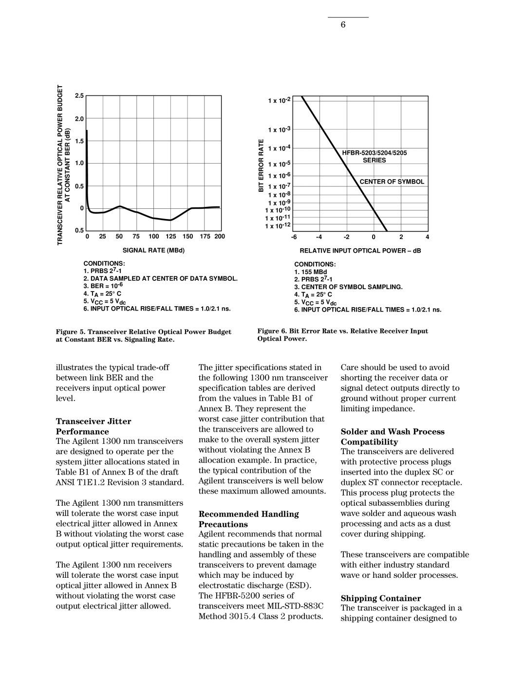
Figure 5. Transceiver Relative Optical Power Budget at Constant BER vs. Signaling Rate.
Figure 6. Bit Error Rate vs. Relative Receiver Input Optical Power.
illustrates the typical
Transceiver Jitter
Performance
The Agilent 1300 nm transceivers are designed to operate per the system jitter allocations stated in Table B1 of Annex B of the draft ANSI T1E1.2 Revision 3 standard.
The Agilent 1300 nm transmitters will tolerate the worst case input electrical jitter allowed in Annex B without violating the worst case output optical jitter requirements.
The Agilent 1300 nm receivers will tolerate the worst case input optical jitter allowed in Annex B without violating the worst case output electrical jitter allowed.
The jitter specifications stated in the following 1300 nm transceiver specification tables are derived from the values in Table B1 of Annex B. They represent the worst case jitter contribution that the transceivers are allowed to make to the overall system jitter without violating the Annex B allocation example. In practice, the typical contribution of the Agilent transceivers is well below these maximum allowed amounts.
Recommended Handling Precautions
Agilent recommends that normal static precautions be taken in the handling and assembly of these transceivers to prevent damage which may be induced by electrostatic discharge (ESD). The
Care should be used to avoid shorting the receiver data or signal detect outputs directly to ground without proper current limiting impedance.
Solder and Wash Process Compatibility
The transceivers are delivered with protective process plugs inserted into the duplex SC or duplex ST connector receptacle. This process plug protects the optical subassemblies during wave solder and aqueous wash processing and acts as a dust cover during shipping.
These transceivers are compatible with either industry standard wave or hand solder processes.