2
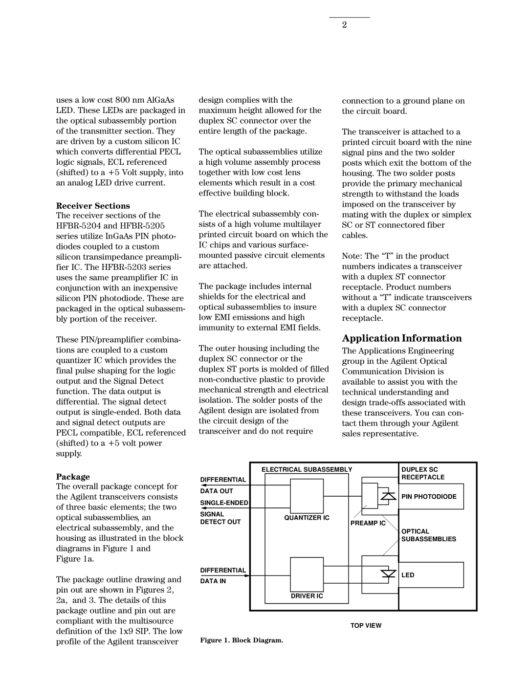
uses a low cost 800 nm AlGaAs LED. These LEDs are packaged in the optical subassembly portion of the transmitter section. They are driven by a custom silicon IC which converts differential PECL logic signals, ECL referenced (shifted) to a +5 Volt supply, into an analog LED drive current.
Receiver Sections
The receiver sections of the
design complies with the maximum height allowed for the duplex SC connector over the entire length of the package.
The optical subassemblies utilize a high volume assembly process together with low cost lens elements which result in a cost effective building block.
The electrical subassembly con- sists of a high volume multilayer printed circuit board on which the IC chips and various surface- mounted passive circuit elements are attached.
The package includes internal shields for the electrical and optical subassemblies to insure low EMI emissions and high immunity to external EMI fields.
connection to a ground plane on the circuit board.
The transceiver is attached to a printed circuit board with the nine signal pins and the two solder posts which exit the bottom of the housing. The two solder posts provide the primary mechanical strength to withstand the loads imposed on the transceiver by mating with the duplex or simplex SC or ST connectored fiber cables.
Note: The “T” in the product numbers indicates a transceiver with a duplex ST connector receptacle. Product numbers without a “T” indicate transceivers with a duplex SC connector receptacle.
These PIN/preamplifier combina- tions are coupled to a custom quantizer IC which provides the final pulse shaping for the logic output and the Signal Detect function. The data output is differential. The signal detect output is
The outer housing including the duplex SC connector or the duplex ST ports is molded of filled
Application Information
The Applications Engineering group in the Agilent Optical Communication Division is available to assist you with the technical understanding and design
Package
The overall package concept for the Agilent transceivers consists of three basic elements; the two optical subassemblies, an electrical subassembly, and the housing as illustrated in the block diagrams in Figure 1 and Figure 1a.
The package outline drawing and pin out are shown in Figures 2, 2a, and 3. The details of this package outline and pin out are compliant with the multisource definition of the 1x9 SIP. The low profile of the Agilent transceiver
| ELECTRICAL SUBASSEMBLY | DUPLEX SC |
DIFFERENTIAL |
| RECEPTACLE |
|
| |
DATA OUT |
| PIN PHOTODIODE |
| ||
|
| |
SIGNAL | QUANTIZER IC |
|
DETECT OUT |
| |
PREAMP IC |
| |
|
| OPTICAL |
|
| SUBASSEMBLIES |
DIFFERENTIAL |
| LED |
DATA IN |
| |
|
| |
| DRIVER IC |
|
TOP VIEW