|
|
|
|
|
|
| 8 |
|
|
| (2X) ø | 1.9 ± 0.1 |
|
| |
|
| 20.32 | .075 ± .004 | ||||
|
|
|
|
|
| ||
|
| Ø0.000 | M | A |
| ||
|
| .800 |
| ||||
|
|
|
|
|
|
| |
20.32 |
| (9X) ø | 0.8 ± 0.1 |
|
| ||
| .032 ± .004 |
| |||||
.800 |
|
|
|
|
|
| |
|
|
| Ø0.000 | M | A |
| |
(8X) | 2.54 |
|
|
|
|
|
|
| .100 |
|
|
|
|
|
|
|
|
| TOP VIEW |
|
|
|
|
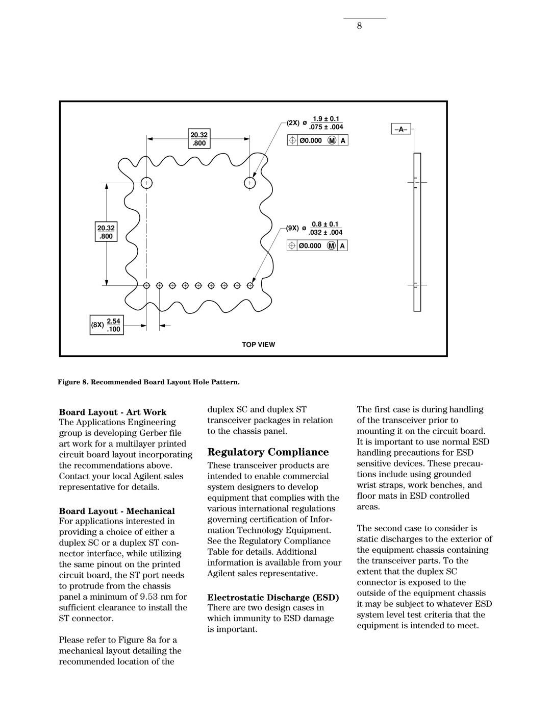
Figure 8. Recommended Board Layout Hole Pattern.
Board Layout - Art Work The Applications Engineering group is developing Gerber file art work for a multilayer printed circuit board layout incorporating the recommendations above. Contact your local Agilent sales representative for details.
Board Layout - Mechanical For applications interested in providing a choice of either a duplex SC or a duplex ST con- nector interface, while utilizing the same pinout on the printed circuit board, the ST port needs to protrude from the chassis panel a minimum of 9.53 nm for sufficient clearance to install the ST connector.
Please refer to Figure 8a for a mechanical layout detailing the recommended location of the
duplex SC and duplex ST transceiver packages in relation to the chassis panel.
Regulatory Compliance
These transceiver products are intended to enable commercial system designers to develop equipment that complies with the various international regulations governing certification of Infor- mation Technology Equipment. See the Regulatory Compliance Table for details. Additional information is available from your Agilent sales representative.
Electrostatic Discharge (ESD) There are two design cases in which immunity to ESD damage is important.
The first case is during handling of the transceiver prior to mounting it on the circuit board. It is important to use normal ESD handling precautions for ESD sensitive devices. These precau- tions include using grounded wrist straps, work benches, and floor mats in ESD controlled areas.
The second case to consider is static discharges to the exterior of the equipment chassis containing the transceiver parts. To the extent that the duplex SC connector is exposed to the outside of the equipment chassis it may be subject to whatever ESD system level test criteria that the equipment is intended to meet.