15
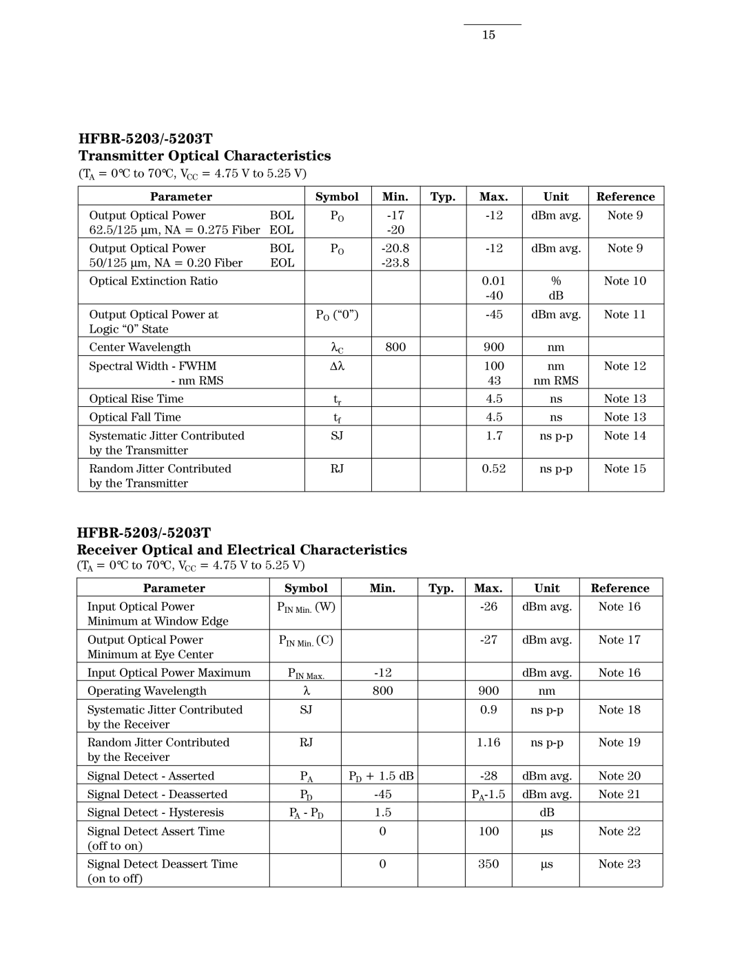
HFBR-5203/-5203T
Transmitter Optical Characteristics (TA = 0°C to 70°C, VCC = 4.75 V to 5.25 V)
Parameter |
| Symbol | Min. | Typ. | Max. | Unit | Reference |
|
|
|
|
|
|
|
|
Output Optical Power | BOL | PO |
| dBm avg. | Note 9 | ||
62.5/125 μm, NA = 0.275 Fiber | EOL |
|
|
|
|
| |
Output Optical Power | BOL | PO |
| dBm avg. | Note 9 | ||
50/125 μm, NA = 0.20 Fiber | EOL |
|
|
|
|
| |
Optical Extinction Ratio |
|
|
|
| 0.01 | % | Note 10 |
|
|
|
|
| dB |
| |
Output Optical Power at |
| PO (“0”) |
|
| dBm avg. | Note 11 | |
Logic “0” State |
|
|
|
|
|
|
|
Center Wavelength |
| λC | 800 |
| 900 | nm |
|
Spectral Width - FWHM |
| Δλ |
|
| 100 | nm | Note 12 |
- nm RMS |
|
|
|
| 43 | nm RMS |
|
Optical Rise Time |
| tr |
|
| 4.5 | ns | Note 13 |
Optical Fall Time |
| tf |
|
| 4.5 | ns | Note 13 |
Systematic Jitter Contributed |
| SJ |
|
| 1.7 | ns | Note 14 |
by the Transmitter |
|
|
|
|
|
|
|
Random Jitter Contributed |
| RJ |
|
| 0.52 | ns | Note 15 |
by the Transmitter |
|
|
|
|
|
|
|
HFBR-5203/-5203T
Receiver Optical and Electrical Characteristics (TA = 0°C to 70°C, VCC = 4.75 V to 5.25 V)
Parameter | Symbol | Min. | Typ. | Max. | Unit | Reference |
Input Optical Power | PIN Min. (W) |
|
| dBm avg. | Note 16 | |
Minimum at Window Edge |
|
|
|
|
|
|
Output Optical Power | PIN Min. (C) |
|
| dBm avg. | Note 17 | |
Minimum at Eye Center |
|
|
|
|
|
|
Input Optical Power Maximum | PIN Max. |
|
| dBm avg. | Note 16 | |
Operating Wavelength | λ | 800 |
| 900 | nm |
|
Systematic Jitter Contributed | SJ |
|
| 0.9 | ns | Note 18 |
by the Receiver |
|
|
|
|
|
|
Random Jitter Contributed | RJ |
|
| 1.16 | ns | Note 19 |
by the Receiver |
|
|
|
|
|
|
|
|
|
|
|
|
|
Signal Detect - Asserted | PA | PD + 1.5 dB |
| dBm avg. | Note 20 | |
Signal Detect - Deasserted | PD |
| dBm avg. | Note 21 | ||
Signal Detect - Hysteresis | PA - PD | 1.5 |
|
| dB |
|
Signal Detect Assert Time |
| 0 |
| 100 | μs | Note 22 |
(off to on) |
|
|
|
|
|
|
Signal Detect Deassert Time |
| 0 |
| 350 | μs | Note 23 |
(on to off) |
|
|
|
|
|
|