18
HFBR-5205/-5205T
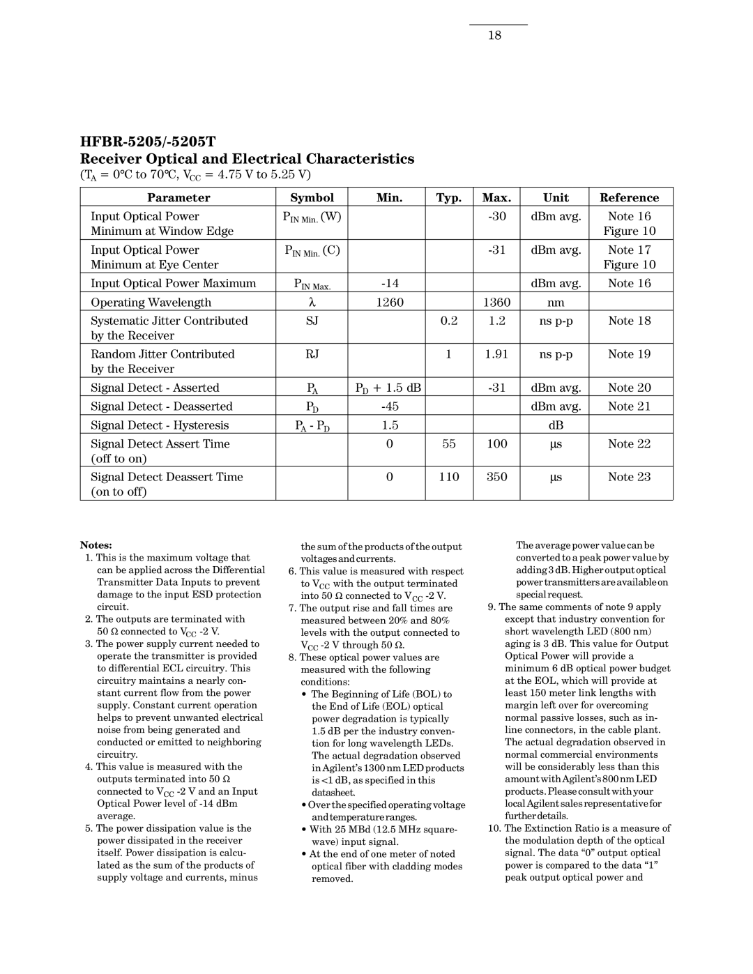
Receiver Optical and Electrical Characteristics (TA = 0°C to 70°C, VCC = 4.75 V to 5.25 V)
Parameter | Symbol | Min. | Typ. | Max. | Unit | Reference |
Input Optical Power | PIN Min. (W) |
|
| dBm avg. | Note 16 | |
Minimum at Window Edge |
|
|
|
|
| Figure 10 |
Input Optical Power | PIN Min. (C) |
|
| dBm avg. | Note 17 | |
Minimum at Eye Center |
|
|
|
|
| Figure 10 |
Input Optical Power Maximum | PIN Max. |
|
| dBm avg. | Note 16 | |
Operating Wavelength | λ | 1260 |
| 1360 | nm |
|
Systematic Jitter Contributed | SJ |
| 0.2 | 1.2 | ns | Note 18 |
by the Receiver |
|
|
|
|
|
|
Random Jitter Contributed | RJ |
| 1 | 1.91 | ns | Note 19 |
by the Receiver |
|
|
|
|
|
|
|
|
|
|
|
|
|
Signal Detect - Asserted | PA | PD + 1.5 dB |
| dBm avg. | Note 20 | |
Signal Detect - Deasserted | PD |
|
| dBm avg. | Note 21 | |
Signal Detect - Hysteresis | PA - PD | 1.5 |
|
| dB |
|
Signal Detect Assert Time |
| 0 | 55 | 100 | μs | Note 22 |
(off to on) |
|
|
|
|
|
|
Signal Detect Deassert Time |
| 0 | 110 | 350 | μs | Note 23 |
(on to off) |
|
|
|
|
|
|
|
|
|
|
|
|
|
Notes:
1.This is the maximum voltage that can be applied across the Differential Transmitter Data Inputs to prevent damage to the input ESD protection circuit.
2.The outputs are terminated with
50 Ω connected to VCC
3.The power supply current needed to operate the transmitter is provided to differential ECL circuitry. This circuitry maintains a nearly con- stant current flow from the power supply. Constant current operation helps to prevent unwanted electrical noise from being generated and conducted or emitted to neighboring circuitry.
4.This value is measured with the outputs terminated into 50 Ω
connected to VCC
5.The power dissipation value is the power dissipated in the receiver itself. Power dissipation is calcu- lated as the sum of the products of supply voltage and currents, minus
the sum of the products of the output voltagesandcurrents.
6.This value is measured with respect
to VCC with the output terminated into 50 Ω connected to VCC
7.The output rise and fall times are measured between 20% and 80% levels with the output connected to
VCC
8.These optical power values are measured with the following conditions:
•The Beginning of Life (BOL) to the End of Life (EOL) optical power degradation is typically
1.5 dB per the industry conven- tion for long wavelength LEDs. The actual degradation observed in Agilent’s 1300 nm LED products is <1 dB, as specified in this datasheet.
•Over the specified operating voltage andtemperatureranges.
•With 25 MBd (12.5 MHz square- wave) input signal.
•At the end of one meter of noted optical fiber with cladding modes removed.
The average power value can be converted to a peak power value by adding 3 dB. Higher output optical powertransmittersareavailableon specialrequest.
9.The same comments of note 9 apply except that industry convention for short wavelength LED (800 nm) aging is 3 dB. This value for Output Optical Power will provide a minimum 6 dB optical power budget at the EOL, which will provide at least 150 meter link lengths with margin left over for overcoming normal passive losses, such as in- line connectors, in the cable plant. The actual degradation observed in normal commercial environments will be considerably less than this amount with Agilent’s 800 nm LED products. Please consult with your local Agilent sales representative for furtherdetails.
10.The Extinction Ratio is a measure of the modulation depth of the optical signal. The data “0” output optical power is compared to the data “1” peak output optical power and