7
NO INTERNAL CONNECTION | NO INTERNAL CONNECTION |
TOP VIEW
Rx |
|
|
|
| Rx | Tx |
|
| Tx |
VEE | RD | RD | SD | VCC | VCC | TD | TD | VEE | |
1 | 2 |
| 3 | 4 | 5 | 6 | 7 | 8 | 9 |
|
|
|
|
| C1 |
| C2 |
|
|
|
|
|
|
|
|
|
| VCC | |
TERMINATION |
|
|
|
| L1 | L2 |
| R2 | R3 |
|
|
|
|
|
|
|
|
| |
AT PHY |
|
|
|
|
|
|
| R1 | R4 |
DEVICE |
| VCC |
| C3 | C4 |
| |||
INPUTS | R5 |
| R7 |
| VCC FILTER |
|
| C5 | |
|
|
|
|
|
| ||||
|
|
|
|
| AT VCC PINS |
|
|
| |
|
|
|
|
| TRANSCEIVER | TERMINATION | |||
|
|
| C6 |
| R9 |
|
| ||
R6 |
|
|
|
|
| AT TRANSCEIVER | |||
|
| R8 |
|
|
|
| |||
|
|
|
|
| R10 |
|
| INPUTS |
|
|
|
|
|
|
|
|
|
| |
| RD |
| RD | SD | VCC |
| TD | TD | |
NOTES:
THE
R1 = R4 = R6 = R8 = R10 = 130 OHMS.
R2 = R3 = R5 = R7 = R9 = 82 OHMS.
C1 = C2 = C3 = C5 = C6 = 0.1 µF.
C4 = 10 µF.
L1 = L2 = 1 µH COIL OR FERRITE INDUCTOR.
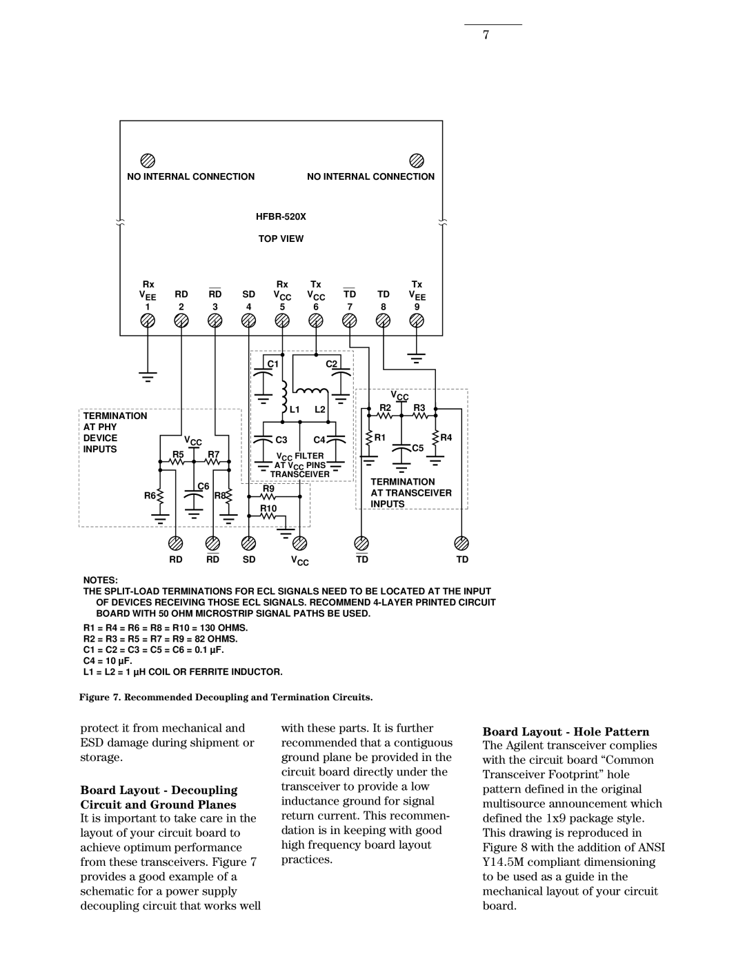
Figure 7. Recommended Decoupling and Termination Circuits.
protect it from mechanical and ESD damage during shipment or storage.
Board Layout - Decoupling Circuit and Ground Planes
It is important to take care in the layout of your circuit board to achieve optimum performance from these transceivers. Figure 7 provides a good example of a schematic for a power supply decoupling circuit that works well
with these parts. It is further recommended that a contiguous ground plane be provided in the circuit board directly under the transceiver to provide a low inductance ground for signal return current. This recommen- dation is in keeping with good high frequency board layout practices.
Board Layout - Hole Pattern The Agilent transceiver complies with the circuit board “Common Transceiver Footprint” hole pattern defined in the original multisource announcement which defined the 1x9 package style. This drawing is reproduced in Figure 8 with the addition of ANSI Y14.5M compliant dimensioning to be used as a guide in the mechanical layout of your circuit board.