Component Location Diagrams
Each foldout includes a component locations diagram with a look-up table for locating electrical components. Figure 4-1 gives the component locations for the Control board and Figure 4-3 gives the component locations for the Power board. The coordinates in the look-up table under each diagram reference the grid on the diagram and give the location of some point on each component to within 1/10 of a unit. The mainframe Service Manual gives several examples of how to use the table.
The component locations diagram also indicates specific troubleshooting test point locations. The test points are described in Chapter 3 of the mainframe Service Manual and are used in various troubleshooting procedures described in that chapter.

4

Diagrams

Schematic Diagrams

Schematic diagrams and component location diagrams are provided for the Control board as well as the Power board on two foldout pages. Two schematic diagrams of the Power board are included in Figure 4-2 on the first foldout; three schematic diagrams of the Control board are included in Figure 4-4 on the second foldout. Table 4-1 lists the notes that apply to both the Control board and Power board schematic diagrams.

Table 4-2 lists, alphabetically, all of the signal names that appear on the schematic, along with a brief description of the signal's function. To help you locate where signals come from and go to, Table 4-1 lists the coordinates for each appearance of a signal on each sheet of the schematic. Coordinates printed in BOLD indicate the signal origin. On the Control board for example, when ACLR* is active, it clears the analog circuits. ACLR* originates in area 4D of sheet 1 and also appears in area 2B of sheet 3.

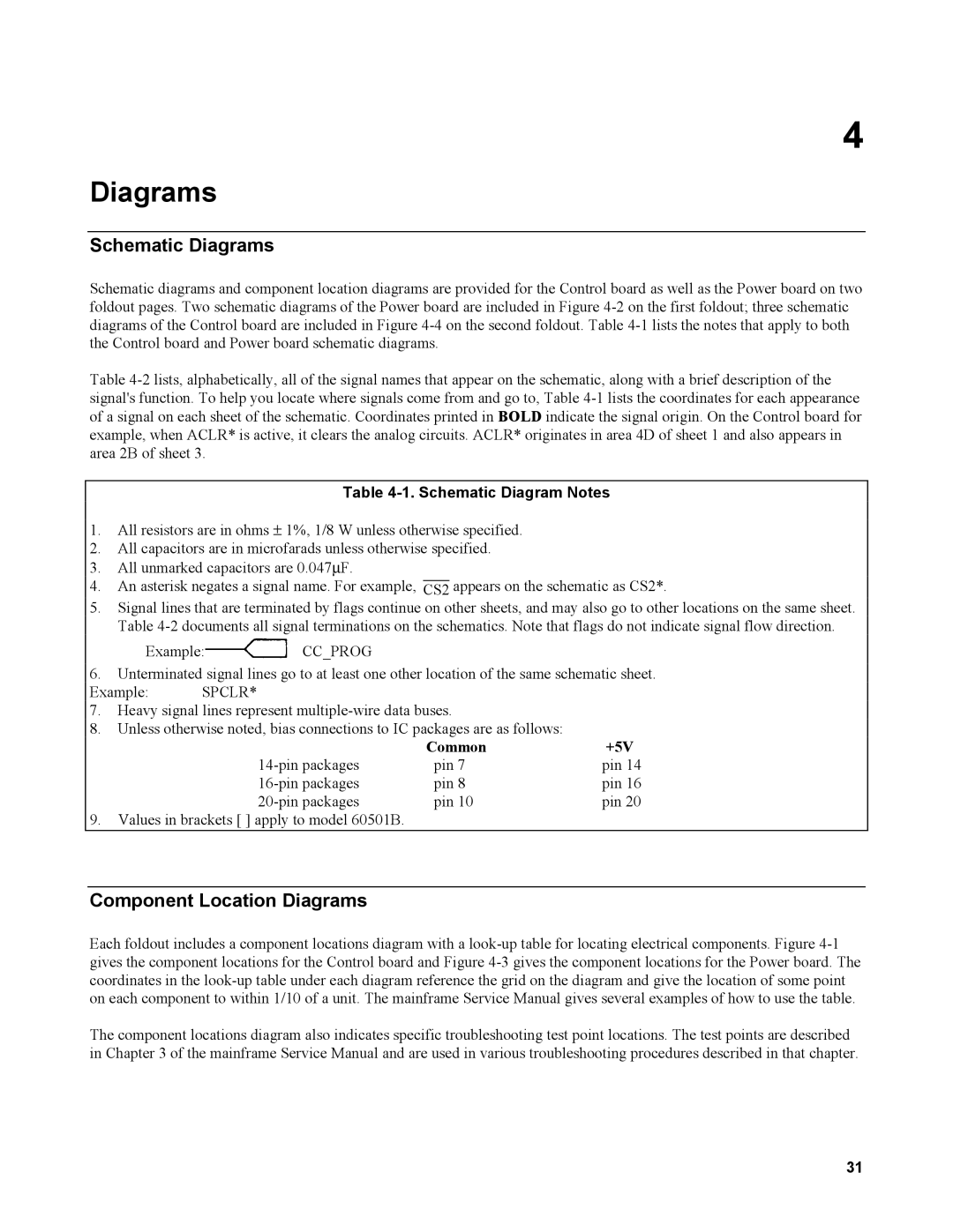
Table 4-1. Schematic Diagram Notes

1.All resistors are in ohms ± 1%, 1/8 W unless otherwise specified.

2.All capacitors are in microfarads unless otherwise specified.

3.All unmarked capacitors are 0.047∝F.

4.An asterisk negates a signal name. For example, CS2 appears on the schematic as CS2*.

5.Signal lines that are terminated by flags continue on other sheets, and may also go to other locations on the same sheet. Table 4-2 documents all signal terminations on the schematics. Note that flags do not indicate signal flow direction.

Example: CC_PROG

6.Unterminated signal lines go to at least one other location of the same schematic sheet.

Example: SPCLR*

7.Heavy signal lines represent multiple-wire data buses.

8.Unless otherwise noted, bias connections to IC packages are as follows:


Common

+5V

14-pin packages

pin 7

pin 14

16-pin packages

pin 8

pin 16

20-pin packages

pin 10

pin 20

9. Values in brackets [ ] apply to model 60501B.


31

Page 31
Image 31
Agilent Technologies 60502B, 60501B service manual Schematic Diagrams, Schematic Diagram Notes, Common +5V

60501B, 60502B specifications

Agilent Technologies 60502B is a high-performance signal generator designed for a wide range of applications, including aerospace, telecommunications, and research and development. As part of Agilent's advanced suite of test and measurement solutions, the 60502B provides users with the capability to generate high-quality signals with exceptional accuracy and stability.

One of the standout features of the Agilent 60502B is its frequency range, which spans from 9 kHz to 6 GHz. This broad range enables engineers and technicians to work with various modulation formats and signal types, making it highly versatile for testing and development. The generator supports continuous wave (CW) signals as well as complex modulated signals, accommodating both narrowband and broadband applications.

The 60502B employs advanced direct digital synthesis (DDS) technology, ensuring accurate frequency generation with low phase noise. This technology is essential for applications that require high precision and minimal signal distortion, such as radar and communication systems. The generator’s phase noise performance is exceptional, which enhances its capability for demanding applications requiring signal integrity.

Another key characteristic of the Agilent 60502B is its output power handling. It can deliver output levels ranging from -130 dBm up to +10 dBm, enabling users to drive various loads and achieve optimal testing conditions. This flexibility is particularly beneficial in laboratory environments where different power levels are needed for different devices under test.

The user interface of the 60502B is designed for efficiency and ease of use. It incorporates a large display that provides real-time feedback on settings and signal characteristics, facilitating quick adjustments during testing. Furthermore, the generator is equipped with USB and GPIB interfaces, enabling seamless integration into automated test systems and easy connectivity to computers for remote control and data logging.

In addition to its robust hardware features, the Agilent 60502B supports a variety of modulation schemes, including AM, FM, PM, and pulse modulation. This capability allows users to simulate real-world signals and assess the performance of receivers and other components under various conditions.

Overall, the Agilent Technologies 60502B signal generator stands out in terms of performance, versatility, and user-friendliness. Its wide frequency range, advanced DDS technology, significant power output capabilities, and support for multiple modulation types make it an indispensable tool for engineers across various industries engaged in testing and development activities. Whether for research projects or routine maintenance tasks, the 60502B is built to deliver reliable and precise results.