Operational Considerations
Calibration time
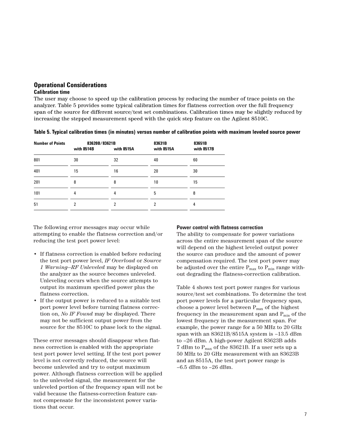
The user may choose to speed up the calibration process by reducing the number of trace points on the analyzer. Table 5 provides some typical calibration times for flatness correction over the full frequency span of the source for different source/test set combinations. Calibration times may be slightly reduced by increasing the stepped measurement speed with the quick step feature on the Agilent 8510C.
Table 5. Typical calibration times (in minutes) versus number of calibration points with maximum leveled source power
Number of Points | 83620B/83621B | 83631B | 83651B | |
| with 8514B | with 8515A | with 8515A | with 8517B |
|
|
|
|
|
801 | 30 | 32 | 40 | 60 |
|
|
|
|
|
401 | 15 | 16 | 20 | 30 |
|
|
|
|
|
201 | 8 | 8 | 10 | 15 |
|
|
|
|
|
101 | 4 | 4 | 5 | 8 |
|
|
|
|
|
51 | 2 | 2 | 2 | 4 |
|
|
|
|
|
The following error messages may occur while attempting to enable the flatness correction and/or reducing the test port power level:
•If flatness correction is enabled before reducing the test port power level, IF Overload or Source 1
•If the output power is reduced to a suitable test port power level before turning flatness correc- tion on, No IF Found may be displayed. There may not be sufficient output power from the source for the 8510C to phase lock to the signal.
These error messages should disappear when flat- ness correction is enabled with the appropriate test port power level setting. If the test port power level is not correctly reduced, the source will become unleveled and try to output maximum power. Although flatness correction will be applied to the unleveled signal, the measurement for the unleveled portion of the frequency span will not be valid because the
Power control with flatness correction
The ability to compensate for power variations across the entire measurement span of the source will depend on the highest leveled output power the source can produce and the amount of power compensation required. The test port power may be adjusted over the entire Pmax to Pmin range with- out degrading the
Table 4 shows test port power ranges for various source/test set combinations. To determine the test port power levels for a particular frequency span, choose a power level between Pmax of the highest frequency in the measurement span and Pmin of the lowest frequency in the measurement span. For example, the power range for a 50 MHz to 20 GHz span with an 83621B/8515A system is
7 dBm to Pmax of the 83621B. If a user sets up a
50 MHz to 20 GHz measurement with an 83623B and an 8515A, the test port power range is
7