AD9883A
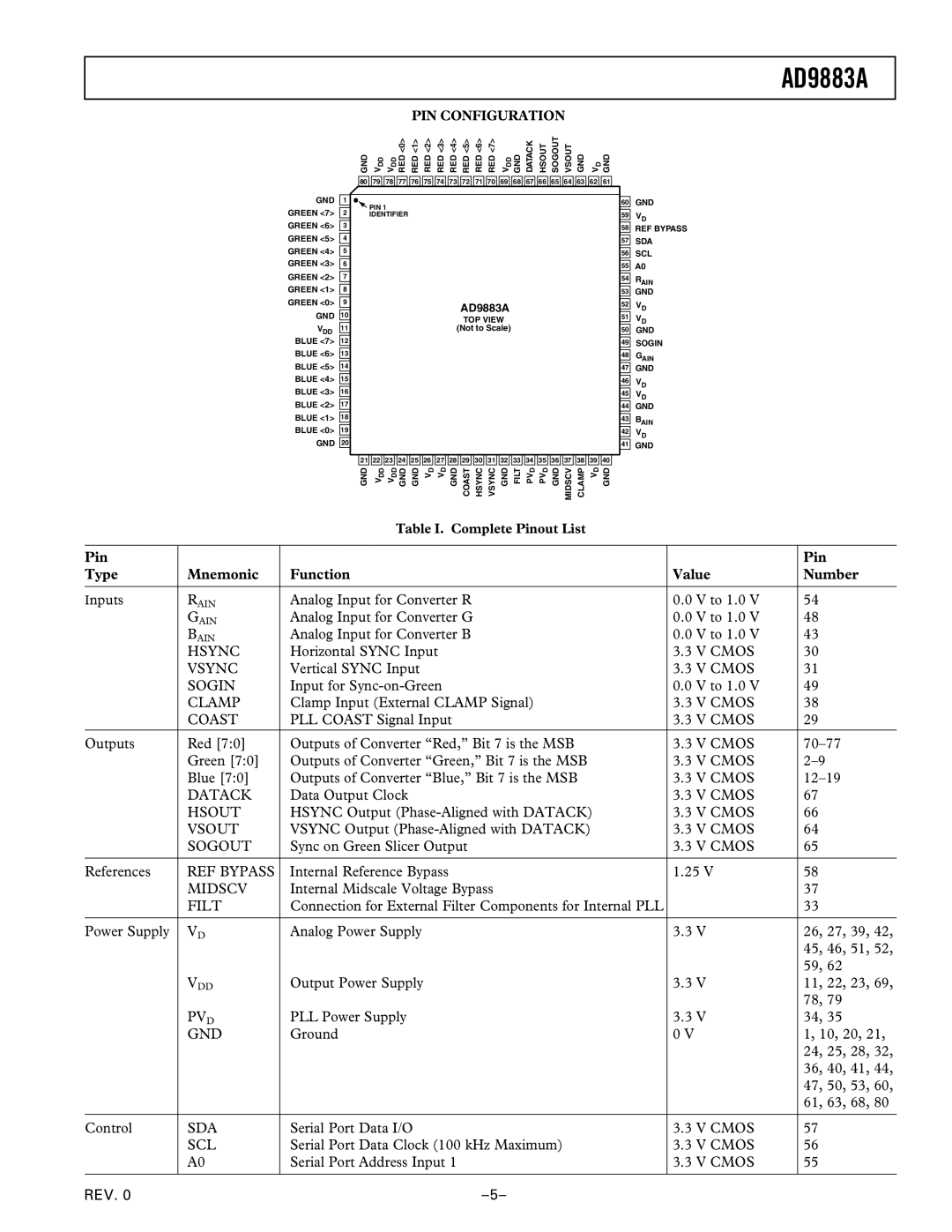
PIN CONFIGURATION
GND GREEN <7> GREEN <6> GREEN <5> GREEN <4> GREEN <3> GREEN <2> GREEN <1> GREEN <0>
GND
VDD
BLUE <7> BLUE <6> BLUE <5> BLUE <4> BLUE <3> BLUE <2> BLUE <1> BLUE <0>
GND
|
| GND | V | V | RED<0> | RED<1> | RED<2> | RED<3> | RED<4> | RED<5> | RED<6> | RED<7> | V | GND | DATACK | HSOUT | SOGOUT | VSOUT | GND | V | GND |
|
|
|
| DD | DD |
|
|
|
|
|
|
|
| DD |
|
|
|
|
|
| D |
|
|
|
| 80 | 79 | 78 | 77 | 76 | 75 | 74 | 73 | 72 | 71 | 70 | 69 | 68 | 67 | 66 | 65 | 64 | 63 | 62 | 61 |
|
|
|
|
|
|
|
|
|
|
|
|
|
|
|
|
|
|
|
|
|
|
|
|
1 |
|
| PIN 1 |
|
|
|
|
|
|
|
|
|
|
|
|
|
|
|
|
|
| |
|
|
|
|
|
|
|
|
|
|
|
|
|
|
|
|
|
|
|
|
| ||
2 |
|
| IDENTIFIER |
|
|
|
|
|
|
|
|
|
|
|
|
|
|
|
|
| ||
|
|
|
|
|
|
|
|
|
|
|
|
|
|
|
|
|
|
|
|
|
|
|
3 |
|
|
|
|
|
|
|
|
|
|
|
|
|
|
|
|
|
|
|
|
|
|
|
|
|
|
|
|
|
|
|
|
|
|
|
|
|
|
|
|
|
|
|
|
|
4 |
|
|
|
|
|
|
|
|
|
|
|
|
|
|
|
|
|
|
|
|
|
|
|
|
|
|
|
|
|
|
|
|
|
|
|
|
|
|
|
|
|
|
|
|
|
5 |
|
|
|
|
|
|
|
|
|
|
|
|
|
|
|
|
|
|
|
|
|
|
|
|
|
|
|
|
|
|
|
|
|
|
|
|
|
|
|
|
|
|
|
|
|
6 |
|
|
|
|
|
|
|
|
|
|
|
|
|
|
|
|
|
|
|
|
|
|
|
|
|
|
|
|
|
|
|
|
|
|
|
|
|
|
|
|
|
|
|
|
|
7 |
|
|
|
|
|
|
|
|
|
|
|
|
|
|
|
|
|
|
|
|
|
|
|
|
|
|
|
|
|
|
|
|
|
|
|
|
|
|
|
|
|
|
|
|
|
8 |
|
|
|
|
|
|
|
|
|
|
|
|
|
|
|
|
|
|
|
|
|
|
|
|
|
|
|
|
|
|
|
|
|
|
|
|
|
|
|
|
|
|
|
|
|
9 |
|
|
|
|
|
|
|
|
| AD9883A |
|
|
|
|
|
|
|
|
| |||
|
|
|
|
|
|
|
|
|
|
|
|
|
|
|
|
|
|
| ||||
10 |
|
|
|
|
|
|
|
|
| TOP VIEW |
|
|
|
|
|
|
|
|
| |||
|
|
|
|
|
|
|
|
|
|
|
|
|
|
|
|
|
|
| ||||
11 |
|
|
|
|
|
|
|
| (Not to Scale) |
|
|
|
|
|
|
|
|
| ||||
|
|
|
|
|
|
|
|
|
|
|
|
|
|
|
|
|
|
|
|
|
|
|
12 |
|
|
|
|
|
|
|
|
|
|
|
|
|
|
|
|
|
|
|
|
|
|
|
|
|
|
|
|
|
|
|
|
|
|
|
|
|
|
|
|
|
|
|
|
|
13 |
|
|
|
|
|
|
|
|
|
|
|
|
|
|
|
|
|
|
|
|
|
|
|
|
|
|
|
|
|
|
|
|
|
|
|
|
|
|
|
|
|
|
|
|
|
14 |
|
|
|
|
|
|
|
|
|
|
|
|
|
|
|
|
|
|
|
|
|
|
|
|
|
|
|
|
|
|
|
|
|
|
|
|
|
|
|
|
|
|
|
|
|
15 |
|
|
|
|
|
|
|
|
|
|
|
|
|
|
|
|
|
|
|
|
|
|
|
|
|
|
|
|
|
|
|
|
|
|
|
|
|
|
|
|
|
|
|
|
|
16 |
|
|
|
|
|
|
|
|
|
|
|
|
|
|
|
|
|
|
|
|
|
|
|
|
|
|
|
|
|
|
|
|
|
|
|
|
|
|
|
|
|
|
|
|
|
17 |
|
|
|
|
|
|
|
|
|
|
|
|
|
|
|
|
|
|
|
|
|
|
|
|
|
|
|
|
|
|
|
|
|
|
|
|
|
|
|
|
|
|
|
|
|
18 |
|
|
|
|
|
|
|
|
|
|
|
|
|
|
|
|
|
|
|
|
|
|
|
|
|
|
|
|
|
|
|
|
|
|
|
|
|
|
|
|
|
|
|
|
|
19 |
|
|
|
|
|
|
|
|
|
|
|
|
|
|
|
|
|
|
|
|
|
|
|
|
|
|
|
|
|
|
|
|
|
|
|
|
|
|
|
|
|
|
|
|
|
20 |
|
|
|
|
|
|
|
|
|
|
|
|
|
|
|
|
|
|
|
|
|
|
|
|
|
|
|
|
|
|
|
|
|
|
|
|
|
|
|
|
|
|
| ||
| 21 | 22 | 23 | 24 | 25 | 26 | 27 | 28 | 29 | 30 | 31 | 32 | 33 | 34 | 35 | 36 | 37 | 38 | 39 | 40 |
| |
|
| GND | DD | DD | GND | GND | D | D | GND | COAST | HSYNC | VSYNC | GND | FILT | D | D | GND | MIDSCV | CLAMP | D | GND |
|
|
| V | V | V | V | PV | PV | V |
| |||||||||||||
60GND
59VD
58REF BYPASS
57SDA
56SCL
55A0
54RAIN
53GND
52VD
51VD
50GND
49SOGIN
48GAIN
47GND
46VD
45VD
44GND
43BAIN
42VD
41GND
Table I. Complete Pinout List
Pin |
|
|
|
| Pin |
Type | Mnemonic | Function | Value | Number | |
|
|
|
|
|
|
Inputs | RAIN | Analog Input for Converter R | 0.0 | V to 1.0 V | 54 |
| GAIN | Analog Input for Converter G | 0.0 | V to 1.0 V | 48 |
| BAIN | Analog Input for Converter B | 0.0 | V to 1.0 V | 43 |
| HSYNC | Horizontal SYNC Input | 3.3 | V CMOS | 30 |
| VSYNC | Vertical SYNC Input | 3.3 | V CMOS | 31 |
| SOGIN | Input for | 0.0 | V to 1.0 V | 49 |
| CLAMP | Clamp Input (External CLAMP Signal) | 3.3 | V CMOS | 38 |
| COAST | PLL COAST Signal Input | 3.3 V CMOS | 29 | |
Outputs | Red [7:0] | Outputs of Converter “Red,” Bit 7 is the MSB | 3.3 V CMOS | ||
| Green [7:0] | Outputs of Converter “Green,” Bit 7 is the MSB | 3.3 | V CMOS | |
| Blue [7:0] | Outputs of Converter “Blue,” Bit 7 is the MSB | 3.3 | V CMOS | |
| DATACK | Data Output Clock | 3.3 V CMOS | 67 | |
| HSOUT | HSYNC Output | 3.3 V CMOS | 66 | |
| VSOUT | VSYNC Output | 3.3 V CMOS | 64 | |
| SOGOUT | Sync on Green Slicer Output | 3.3 | V CMOS | 65 |
|
|
|
|
| |
References | REF BYPASS | Internal Reference Bypass | 1.25 V | 58 | |
| MIDSCV | Internal Midscale Voltage Bypass |
|
| 37 |
| FILT | Connection for External Filter Components for Internal PLL |
|
| 33 |
|
|
|
|
|
|
Power Supply | VD | Analog Power Supply | 3.3 | V | 26, 27, 39, 42, |
|
|
|
|
| 45, 46, 51, 52, |
|
|
|
|
| 59, 62 |
| VDD | Output Power Supply | 3.3 | V | 11, 22, 23, 69, |
|
|
|
|
| 78, 79 |
| PVD | PLL Power Supply | 3.3 | V | 34, 35 |
| GND | Ground | 0 V |
| 1, 10, 20, 21, |
|
|
|
|
| 24, 25, 28, 32, |
|
|
|
|
| 36, 40, 41, 44, |
|
|
|
|
| 47, 50, 53, 60, |
|
|
|
|
| 61, 63, 68, 80 |
|
|
|
|
|
|
Control | SDA | Serial Port Data I/O | 3.3 | V CMOS | 57 |
| SCL | Serial Port Data Clock (100 kHz Maximum) | 3.3 | V CMOS | 56 |
| A0 | Serial Port Address Input 1 | 3.3 | V CMOS | 55 |
|
|
|
|
|
|
REV. 0 |