AD9883A
2-Wire Serial Register Map
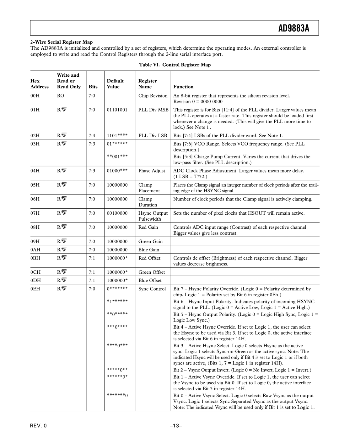
The AD9883A is initialized and controlled by a set of registers, which determine the operating modes. An external controller is employed to write and read the Control Registers through the
Table VI. Control Register Map
| Write and |
|
|
|
|
Hex | Read or |
| Default | Register |
|
Address | Read Only | Bits | Value | Name | Function |
|
|
|
|
|
|
00H | RO | 7:0 |
| Chip Revision | An |
|
|
|
|
| Revision 0 = 0000 0000 |
01H | R/W | 7:0 | 01101001 | PLL Div MSB | This register is for Bits [11:4] of the PLL divider. Larger values mean |
|
|
|
|
| the PLL operates at a faster rate. This register should be loaded first |
|
|
|
|
| whenever a change is needed. (This will give the PLL more time to |
|
|
|
|
| lock.) See Note 1 . |
|
|
|
|
|
|
02H | R/W | 7:4 | 1101**** | PLL Div LSB | Bits [7:4] LSBs of the PLL divider word. See Note 1. |
|
|
|
|
|
|
03H | R/W | 7:3 | 01****** |
| Bits [7:6] VCO Range. Selects VCO frequency range. (See PLL |
|
|
|
|
| description.) |
|
|
| **001*** |
| Bits [5:3] Charge Pump Current. Varies the current that drives the |
|
|
|
|
| |
|
|
|
|
|
|
04H | R/W | 7:3 | 01000*** | Phase Adjust | ADC Clock Phase Adjustment. Larger values mean more delay. |
|
|
|
|
| (1 LSB = T/32.) |
|
|
|
|
|
|
05H | R/W | 7:0 | 10000000 | Clamp | Places the Clamp signal an integer number of clock periods after the trail- |
|
|
|
| Placement | ing edge of the HSYNC signal. |
|
|
|
|
|
|
06H | R/W | 7:0 | 10000000 | Clamp | Number of clock periods that the Clamp signal is actively clamping. |
|
|
|
| Duration |
|
|
|
|
|
|
|
07H | R/W | 7:0 | 00100000 | Hsync Output | Sets the number of pixel clocks that HSOUT will remain active. |
|
|
|
| Pulsewidth |
|
|
|
|
|
|
|
08H | R/W | 7:0 | 10000000 | Red Gain | Controls ADC input range (Contrast) of each respective channel. |
|
|
|
|
| Bigger values give less contrast. |
|
|
|
|
|
|
09H | R/W | 7:0 | 10000000 | Green Gain |
|
|
|
|
|
|
|
0AH | R/W | 7:0 | 10000000 | Blue Gain |
|
|
|
|
|
|
|
0BH | R/W | 7:1 | 1000000* | Red Offset | Controls dc offset (Brightness) of each respective channel. Bigger |
|
|
|
|
| values decrease brightness. |
|
|
|
|
|
|
0CH | R/W | 7:1 | 1000000* | Green Offset |
|
|
|
|
|
|
|
0DH | R/W | 7:1 | 1000000* | Blue Offset |
|
|
|
|
|
|
|
0EH | R/W | 7:0 | 0******* | Sync Control | Bit 7 – Hsync Polarity Override. (Logic 0 = Polarity determined by |
|
|
|
|
| chip, Logic 1 = Polarity set by Bit 6 in register 0Eh.) |
|
|
| *1****** |
| Bit 6 – Hsync Input Polarity. Indicates polarity of incoming HSYNC |
|
|
|
|
| signal to the PLL. (Logic 0 = Active Low, Logic 1 = Active High.) |
|
|
| **0***** |
| Bit 5 – Hsync Output Polarity. (Logic 0 = Logic High Sync, Logic 1 = |
|
|
|
|
| Logic Low Sync.) |
|
|
| ***0**** |
| Bit 4 – Active Hsync Override. If set to Logic 1, the user can select |
|
|
|
|
| the Hsync to be used via Bit 3. If set to Logic 0, the active interface |
|
|
|
|
| is selected via Bit 6 in register 14H. |
|
|
| ****0*** |
| Bit 3 – Active Hsync Select. Logic 0 selects Hsync as the active |
|
|
|
|
| sync. Logic 1 selects |
|
|
|
|
| indicated Hsync will be used only if Bit 4 is set to Logic 1 or if both |
|
|
|
|
| syncs are active, (Bits 1, 7 = Logic 1 in register 14H). |
|
|
| *****0** |
| Bit 2 – Vsync Output Invert. (Logic 0 = No Invert, Logic 1 = Invert.) |
|
|
| ******0* |
| Bit 1 – Active Vsync Override. If set to Logic 1, the user can select |
|
|
|
|
| the Vsync to be used via Bit 0. If set to Logic 0, the active interface |
|
|
|
|
| is selected via Bit 3 in register 14H. |
|
|
| *******0 |
| Bit 0 – Active Vsync Select. Logic 0 selects Raw Vsync as the output |
|
|
|
|
| Vsync. Logic 1 selects Sync Separated Vsync as the output Vsync. |
|
|
|
|
| Note: The indicated Vsync will be used only if Bit 1 is set to Logic 1. |
REV. 0 |