a | 110 MSPS/140 MSPS Analog Interface for | |
Flat Panel Displays | ||
|
|
|
|
| AD9883A |
|
|
|
FEATURES
140 MSPS Maximum Conversion Rate
300 MHz Analog Bandwidth
0.5 V to 1.0 V Analog Input Range
500ps
3.3 V Power Supply Full Sync Processing
Sync Detect for ”Hot Plugging” Midscale Clamping
Low Power: 500 mW Typical 4:2:2 Output Format Mode
APPLICATIONS
RGB Graphics Processing
LCD Monitors and Projectors
Plasma Display Panels
Scan Converters
Microdisplays
Digital TV
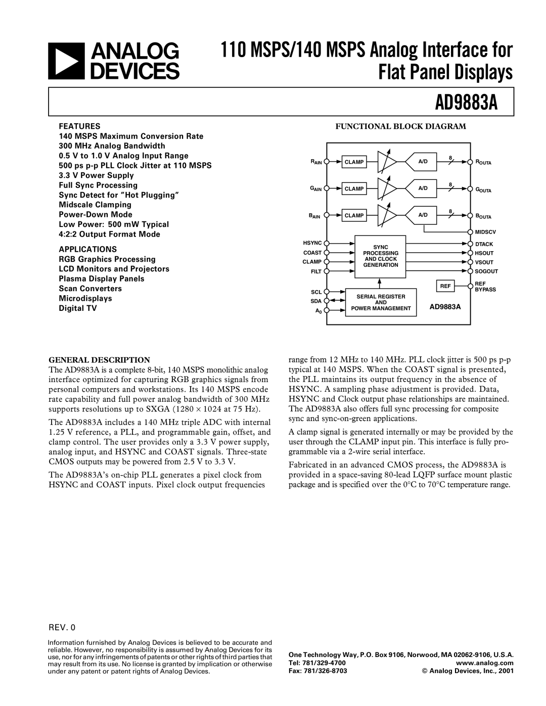
FUNCTIONAL BLOCK DIAGRAM
RAIN | CLAMP | A/D | 8 | ROUTA |
| ||||
GAIN | CLAMP | A/D | 8 | G |
| ||||
|
|
|
| OUTA |
BAIN | CLAMP | A/D | 8 | BOUTA |
| ||||
|
|
|
| MIDSCV |
HSYNC | SYNC |
|
| DTACK |
COAST |
|
|
| |
PROCESSING |
|
| HSOUT | |
CLAMP | AND CLOCK |
|
| VSOUT |
GENERATION |
|
| ||
|
|
|
| |
FILT |
|
|
| SOGOUT |
|
|
| REF | REF |
SCL |
|
| BYPASS | |
|
|
| ||
SERIAL REGISTER |
|
|
| |
SDA |
|
|
| |
AND |
| AD9883A |
| |
A0 | POWER MANAGEMENT |
|
| |
|
|
|
|
GENERAL DESCRIPTION
The AD9883A is a complete
The AD9883A includes a 140 MHz triple ADC with internal
1.25V reference, a PLL, and programmable gain, offset, and clamp control. The user provides only a 3.3 V power supply, analog input, and HSYNC and COAST signals.
The AD9883A’s
range from 12 MHz to 140 MHz. PLL clock jitter is 500 ps
A clamp signal is generated internally or may be provided by the user through the CLAMP input pin. This interface is fully pro- grammable via a
Fabricated in an advanced CMOS process, the AD9883A is provided in a
REV. 0
Information furnished by Analog Devices is believed to be accurate and reliable. However, no responsibility is assumed by Analog Devices for its use, nor for any infringements of patents or other rights of third parties that may result from its use. No license is granted by implication or otherwise under any patent or patent rights of Analog Devices.
One Technology Way, P.O. Box 9106, Norwood, MA
Tel: | www.analog.com |
Fax: | © Analog Devices, Inc., 2001 |
