inverting amplifier, remove R15 and calculate values for R13 and R14 using the equation below.
Gain = VinV0 = 1+ R13R14
NOTE: V0 is the voltage read by the A/D converter chip, and Vin is the voltage at TB1. R13 and R14 should be chosen so that V0 does not exceed 5.00VDC.
0 to 10VDC A/D Input
The 232OPSDA contains one A/D input than is capable of handling voltages between 0VDC and 10VDC. This channel is A/D 3 and is located on Terminal Block 3. The gain of the signal conditioning circuitry for this channel is 0.5. If 10VDC is applied to Terminal Block 3, the A/D Converter chip will read 5.00V. The input resistance of this channel is 200KΩ , so the driving source impedance should be less than 1KΩ to minimize voltage division error.
4-20mA Current Loop A/D Input
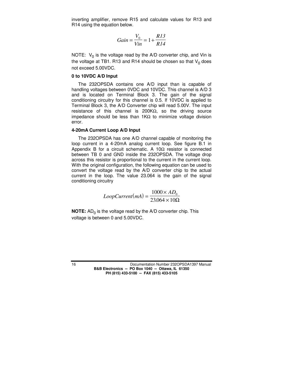
The 232OPSDA has one A/D channel capable of monitoring the loop current in a
( ) |
| 1000 × | AD0 |
LoopCurrent mA | = |
|
|
23.064 | × 10Ω |
NOTE: AD0 is the voltage read by the A/D converter chip. This voltage is between 0 and 5.00VDC.
16Documentation Number 232OPSDA1397 Manual
B&B Electronics
PH (815)