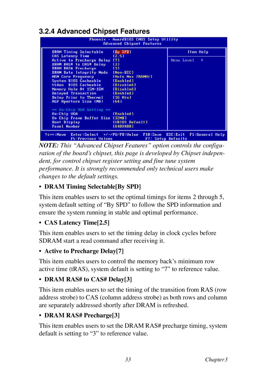
3.2.4 Advanced Chipset Features
NOTE: This “Advanced Chipset Features” option controls the configu- ration of the board’s chipset, this page is developed by Chipset indepen- dent, for control chipset register setting and fine tune system performance. It is strongly recommended only technical users make changes to the default settings.
• DRAM Timing Selectable[By SPD]
This item enables users to set the optimal timings for items 2 through 5, system default setting of “By SPD” to follow the SPD information and ensure the system running in stable and optimal performance.
• CAS Latency Time[2.5]
This item enables users to set the timing delay in clock cycles before SDRAM start a read command after receiving it.
• Active to Precharge Delay[7]
This item enables users to control the memory back’s minimum row active time (tRAS), system default is setting to “7” to reference value.
• DRAM RAS# to CAS# Delay[3]
This item enables users to set the timing of the transition from RAS (row address strobe) to CAS (column address strobe) as both rows and column are separately addressed shortly after DRAM is refreshed.
• DRAM RAS# Precharge[3]
This item enables users to set the DRAM RAS# precharge timing, system default is setting to “3” to reference value.
33 | Chapter3 |
