HARDWARE
2-2 CPCI-824 User’s Manual
Revision 1.0, January 2006
2.3 MEMORY MAP
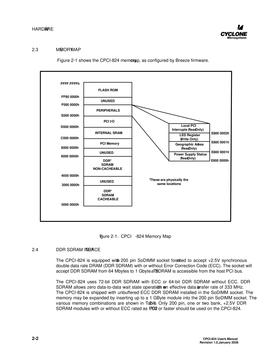
Figure 2-1 shows the CPCI-824 memory map, as configured by Breeze firmware.
Figure 2-1. CPCI-824 Memory Map
2.4 DDR SDRAM INTERFACE
The CPCI-824 is equipped with a 200 pin SoDIMM socket formatted to accept +2.5V synchronous
double data rate DRAM (DDR SDRAM) with or without Error Correction Code (ECC). The socket will
accept DDR SDRAM from 64 Mbytes to 1 Gbyte. The SDRAM is accessible from the host PCI bus.
The CPCI-824 uses 72-bit DDR SDRAM with ECC or 64-bit DDR SDRAM without ECC. DDR
SDRAM allows zero data-to-data wait state operation with an effective data transfer rate of 333 MHz.
The CPCI-824 is shipped with unbuffered ECC DDR SDRAM installed in the SoDIMM socket. The
memory may be expanded by inserting up to a 1 GByte module into the 200 pin SoDIMM socket. The
various memory combinations are shown in Table 2-1. Only 200 pin, one or two bank, +2.5V DDR
SDRAM modules with or without ECC rated as PC2700 or faster should be used on the CPCI-824.
FLASH ROM
UNUSED
PERIPHERALS
PCI I/O
UNUSED
INTERNAL SRAM
PCI Memory
DDR*
SDRAM
NON-CACHEABLE
UNUSED
DDR*
SDRAM
CACHEABLE
Local PCI
Interrupts (Read Only)
LED Register
(Write Only)
Geographic Address
(Read Only)
Power Supply Status
(Read Only)
E800 0002h
E800 0001h
E800 0001h
E800 0000h
* These are physically the
same locations
FFFF FFFFh
FF80 0000h
F000 0000h
E000 0000h
D000 0000h
C000 0000h
8000 0000h
6000 0000h
4000 0000h
2000 0000h
0000 0000h