CY2291
Maximum Ratings
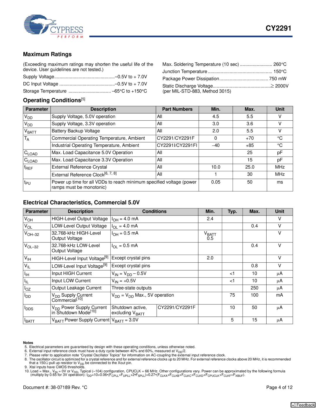
(Exceeding maximum ratings may shorten the useful life of the device. User guidelines are not tested.)
Supply Voltage | |
DC Input Voltage | |
Storage Temperature |
Max. Soldering Temperature (10 sec) | ......................... 260°C |
Junction Temperature | 150°C |
Package Power Dissipation | 750 mW |
Static Discharge Voltage | ≥ 2000V |
(per |
|
Operating Conditions[5]
Parameter | Description | Part Numbers | Min. | Max. | Unit |
VDD | Supply Voltage, 5.0V operation | All | 4.5 | 5.5 | V |
VDD | Supply Voltage, 3.3V operation | All | 3.0 | 3.6 | V |
VBATT | Battery Backup Voltage | All | 2.0 | 5.5 | V |
TA | Commercial Operating Temperature, Ambient | CY2291/CY2291F | 0 | +70 | °C |
| Industrial Operating Temperature, Ambient | CY2291I/CY2291FI | −40 | +85 | °C |
|
|
|
|
|
|
CLOAD | Max. Load Capacitance 5.0V Operation | All |
| 25 | pF |
CLOAD | Max. Load Capacitance 3.3V Operation | All |
| 15 | pF |
fREF | External Reference Crystal | All | 10.0 | 25.0 | MHz |
| External Reference Clock[6, 7, 8] | All | 1 | 30 | MHz |
tPU | Power up time for all VDDs to reach minimum specified voltage (power | 0.05 | 50 | ms | |
| ramps must be monotonic) |
|
|
|
|
Electrical Characteristics, Commercial 5.0V
Parameter | Description | Conditions | Min. | Typ. | Max. | Unit | |
VOH | IOH = 4.0 mA |
| 2.4 |
|
| V | |
VOL | IOL = 4.0 mA |
|
|
| 0.4 | V | |
IOH = 0.5 mA |
| VBATT |
|
| V | ||
| Output Voltage |
|
| 0.5 |
|
|
|
IOL = 0.5 mA |
|
|
| 0.4 | V | ||
| Output Voltage |
|
|
|
|
|
|
VIH | Except crystal pins |
| 2.0 |
|
| V | |
VIL | Except crystal pins |
|
|
| 0.8 | V | |
IIH | Input HIGH Current | VIN = VDD – 0.5V |
|
| <1 | 10 | μA |
IIL | Input LOW Current | VIN = +0.5V |
|
| <1 | 10 | μA |
IOZ | Output Leakage Current |
|
|
| 250 | μA | |
IDD | VDD Supply Current | VDD = VDD Max., 5V operation |
| 75 | 100 | mA | |
| Commercial[10] |
|
|
|
|
|
|
IDDS | VDD Power Supply Current | Shutdown active, | CY2291/CY2291F |
| 10 | 50 | μA |
| in Shutdown Mode[10] | excluding VBATT |
|
|
|
|
|
IBATT | VBATT Power Supply Current | VBATT = 3.0V |
|
| 5 | 15 | μA |
Notes
5.Electrical parameters are guaranteed by design with these operating conditions, unless otherwise noted.
6.External input reference clock must have a duty cycle between 40% and 60%, measured at VDD/2.
7.Please refer to application note “Crystal Oscillator Topics” for information on
8.The oscillator circuit is optimized for a crystal reference and for external reference clocks up to 20 MHz. For external reference clocks above 20 MHz, it is recommended that a 150Ω pull up resistor to VDD be connected to the Xout pin.
9.Xtal inputs have CMOS thresholds.
10.Load = Max., VIN = 0V or VDD, Typical
Document #: | Page 4 of 12 |
[+] Feedback
