|
|
|
|
|
|
|
|
|
|
| CY2291 |
| ||
|
|
|
|
|
|
|
|
|
|
|
|
|
|
|
|
|
|
|
|
|
|
|
|
|
|
|
|
| |
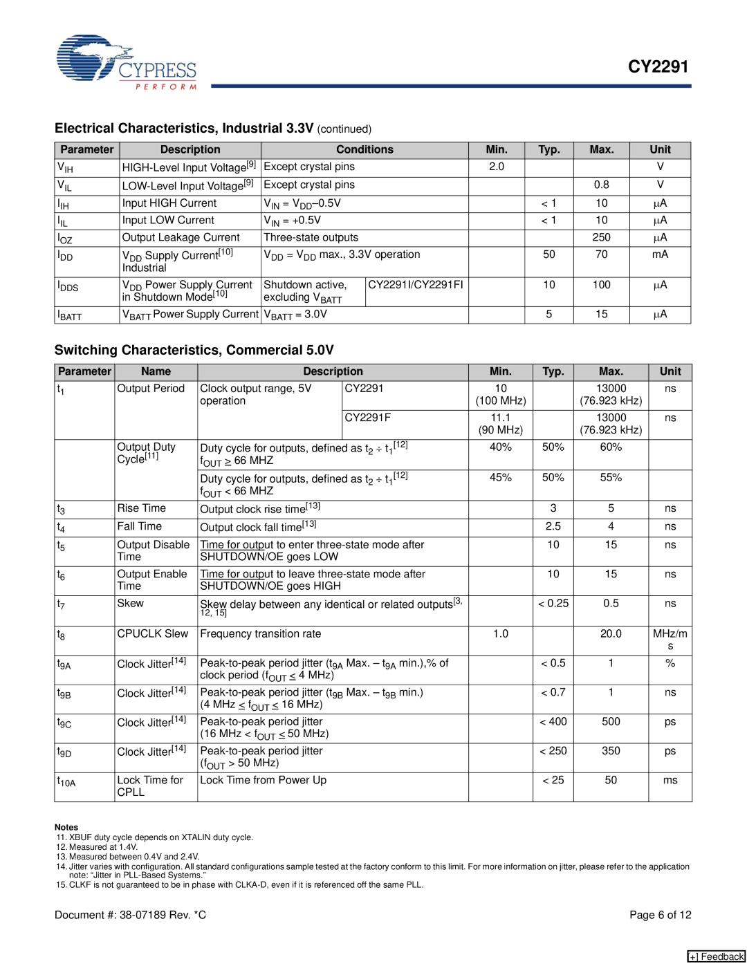
Electrical Characteristics, Industrial 3.3V (continued) |
|
|
|
|
|
|
| |||||||
|
|
|
|
|
|
|
|
|
|
|
|
| ||
Parameter | Description | Conditions | Min. |
| Typ. | Max. |
| Unit |
| |||||
VIH | Except crystal pins |
| 2.0 |
|
|
|
| V |
| |||||
VIL | Except crystal pins |
|
|
|
| 0.8 |
| V |
| |||||
IIH | Input HIGH Current | VIN = |
|
|
|
| < 1 | 10 |
| μA |
| |||
IIL | Input LOW Current | VIN = +0.5V |
|
|
|
| < 1 | 10 |
| μA |
| |||
IOZ | Output Leakage Current |
|
|
|
| 250 |
| μA |
| |||||
IDD | VDD Supply Current[10] | VDD = VDD max., 3.3V operation |
|
| 50 | 70 |
| mA |
| |||||
| Industrial |
|
|
|
|
|
|
|
|
|
|
|
|
|
IDDS | VDD Power Supply Current | Shutdown active, | CY2291I/CY2291FI |
|
| 10 | 100 |
| μA |
| ||||
| in Shutdown Mode[10] | excluding VBATT |
|
|
|
|
|
|
|
|
| |||
IBATT | VBATT Power Supply Current | VBATT = 3.0V |
|
|
|
| 5 | 15 |
| μA |
| |||
Switching Characteristics, Commercial 5.0V |
|
|
|
|
|
|
|
|
| |||||
|
|
|
|
|
|
|
|
|
|
|
|
|
|
|
Parameter | Name |
|
|
| Description |
| Min. | Typ. | Max. | Unit |
| |||
t1 | Output Period | Clock output range, 5V | CY2291 | 10 |
|
| 13000 |
| ns |
| ||||
|
| operation |
|
|
| (100 MHz) |
| (76.923 kHz) |
|
| ||||
|
|
|
|
|
| CY2291F | 11.1 |
|
| 13000 |
| ns |
| |
|
|
|
|
|
|
|
| (90 MHz) |
| (76.923 kHz) |
|
| ||
| Output Duty | Duty cycle for outputs, defined | as t2 ⎟ t1[12] | 40% |
| 50% | 60% |
|
|
| ||||
| Cycle[11] | fOUT > 66 MHZ |
|
|
|
|
|
|
|
|
| |||
|
| Duty cycle for outputs, defined as t2 ⎟ t1[12] | 45% |
| 50% | 55% |
|
|
| |||||
|
| fOUT < 66 MHZ |
|
|
|
|
|
|
|
|
| |||
t3 | Rise Time | Output clock rise time[13] |
|
|
|
| 3 | 5 |
| ns |
| |||
t4 | Fall Time | Output clock fall time[13] |
|
|
|
| 2.5 | 4 |
| ns |
| |||
t5 | Output Disable | Time for output to enter |
|
| 10 | 15 |
| ns |
| |||||
| Time | SHUTDOWN/OE goes LOW |
|
|
|
|
|
|
|
|
| |||
t6 | Output Enable | Time for output to leave |
|
| 10 | 15 |
| ns |
| |||||
| Time | SHUTDOWN/OE goes HIGH |
|
|
|
|
|
|
|
|
| |||
t7 | Skew | Skew delay between any identical or related outputs[3, |
|
| < 0.25 | 0.5 |
| ns |
| |||||
|
| 12, 15] |
|
|
|
|
|
|
|
|
|
| ||
|
|
|
|
|
|
|
|
|
|
|
| |||
t8 | CPUCLK Slew | Frequency transition rate |
|
| 1.0 |
|
| 20.0 |
| MHz/m |
| |||
|
|
|
|
|
|
|
|
|
|
|
|
| s |
|
t9A | Clock Jitter[14] |
|
| < 0.5 | 1 |
| % |
| ||||||
|
| clock period (fOUT < 4 MHz) |
|
|
|
|
|
|
|
|
| |||
t9B | Clock Jitter[14] |
|
| < 0.7 | 1 |
| ns |
| ||||||
|
| (4 MHz < fOUT < 16 MHz) |
|
|
|
|
|
|
|
|
| |||
t9C | Clock Jitter[14] |
|
|
|
| < 400 | 500 |
| ps |
| ||||
|
| (16 MHz < fOUT < 50 MHz) |
|
|
|
|
|
|
|
|
| |||
t9D | Clock Jitter[14] |
|
|
|
| < 250 | 350 |
| ps |
| ||||
|
| (fOUT > 50 MHz) |
|
|
|
|
|
|
|
|
| |||
t10A | Lock Time for | Lock Time from Power Up |
|
|
|
| < 25 | 50 |
| ms |
| |||
| CPLL |
|
|
|
|
|
|
|
|
|
|
|
|
|
Notes
11.XBUF duty cycle depends on XTALIN duty cycle.
12.Measured at 1.4V.
13.Measured between 0.4V and 2.4V.
14.Jitter varies with configuration. All standard configurations sample tested at the factory conform to this limit. For more information on jitter, please refer to the application note: “Jitter in
15.CLKF is not guaranteed to be in phase with
Document #: | Page 6 of 12 |
[+] Feedback
