|
|
|
|
|
|
|
| CY2291 | |
|
|
|
|
|
|
|
|
|
|
|
|
|
|
|
|
|
|
| |
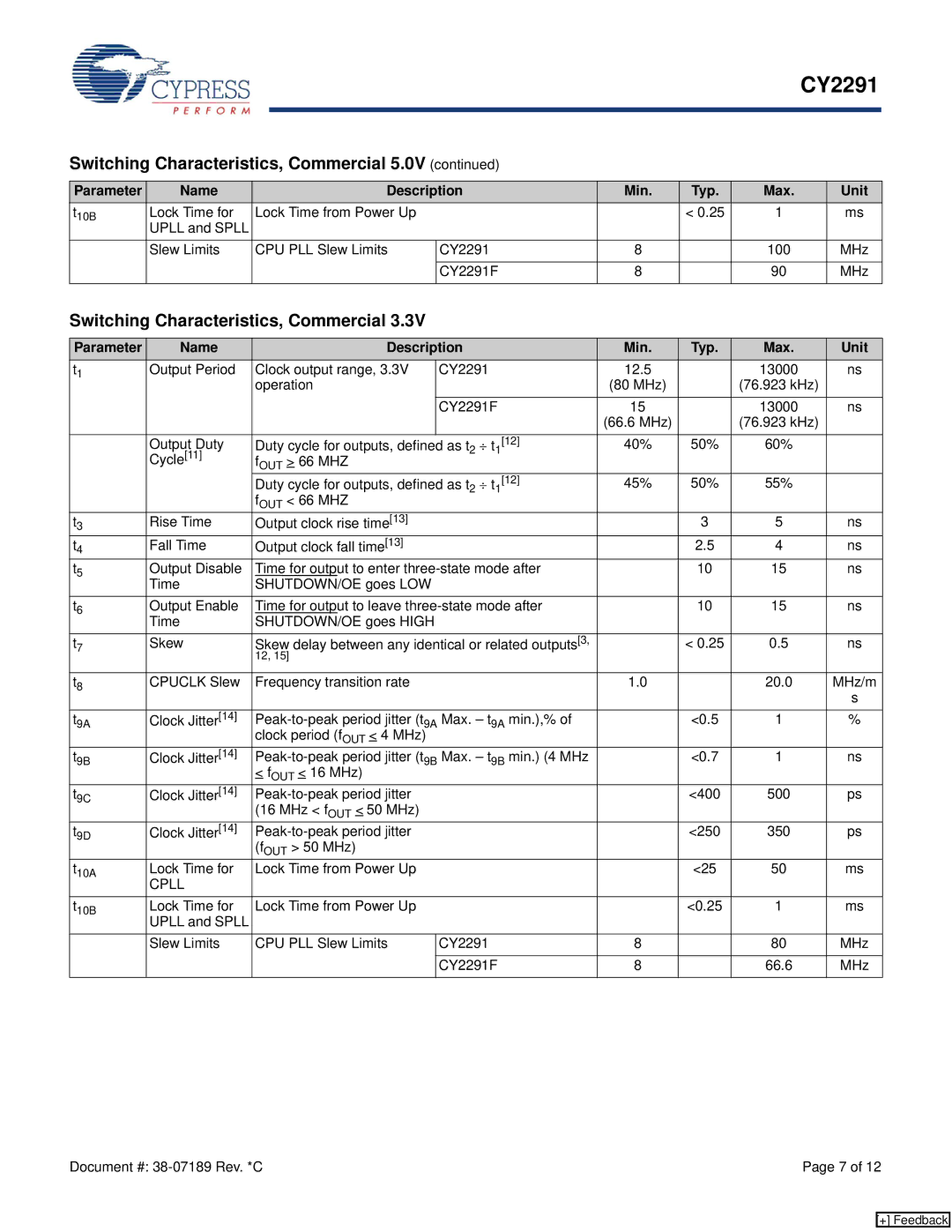
Switching Characteristics, Commercial 5.0V (continued) |
|
|
|
| |||||
|
|
|
|
|
|
|
|
|
|
Parameter | Name |
|
| Description | Min. | Typ. | Max. | Unit | |
t10B | Lock Time for | Lock Time from Power Up |
|
| < 0.25 | 1 | ms | ||
| UPLL and SPLL |
|
|
|
|
|
|
|
|
| Slew Limits | CPU PLL Slew Limits | CY2291 | 8 |
| 100 | MHz | ||
|
|
|
|
|
|
|
|
|
|
|
|
|
|
| CY2291F | 8 |
| 90 | MHz |
|
|
|
|
|
|
|
| ||
Switching Characteristics, Commercial 3.3V |
|
|
|
|
| ||||
|
|
|
|
|
|
|
|
|
|
Parameter | Name |
|
| Description | Min. | Typ. | Max. | Unit | |
t1 | Output Period | Clock output range, 3.3V | CY2291 | 12.5 |
| 13000 | ns | ||
|
| operation |
| (80 MHz) |
| (76.923 kHz) |
| ||
|
|
|
|
| CY2291F | 15 |
| 13000 | ns |
|
|
|
|
|
| (66.6 MHz) |
| (76.923 kHz) |
|
| Output Duty | Duty cycle for outputs, defined | as t2 ⎟ t1[12] | 40% | 50% | 60% |
| ||
| Cycle[11] | fOUT > 66 MHZ |
|
|
|
|
| ||
|
| Duty cycle for outputs, defined as t2 ⎟ t1[12] | 45% | 50% | 55% |
| |||
|
| fOUT < 66 MHZ |
|
|
|
|
| ||
t3 | Rise Time | Output clock rise time[13] |
|
| 3 | 5 | ns | ||
t4 | Fall Time | Output clock fall time[13] |
|
| 2.5 | 4 | ns | ||
t5 | Output Disable | Time for output to enter |
| 10 | 15 | ns | |||
| Time | SHUTDOWN/OE goes LOW |
|
|
|
|
| ||
t6 | Output Enable | Time for output to leave |
| 10 | 15 | ns | |||
| Time | SHUTDOWN/OE goes HIGH |
|
|
|
|
| ||
t7 | Skew | Skew delay between any identical or related outputs[3, |
| < 0.25 | 0.5 | ns | |||
|
| 12, 15] |
|
|
|
|
| ||
|
|
|
|
|
|
|
| ||
t8 | CPUCLK Slew | Frequency transition rate |
| 1.0 |
| 20.0 | MHz/m | ||
|
|
|
|
|
|
|
|
| s |
t9A | Clock Jitter[14] |
| <0.5 | 1 | % | ||||
|
| clock period (fOUT < 4 MHz) |
|
|
|
|
| ||
t9B | Clock Jitter[14] |
| <0.7 | 1 | ns | ||||
|
| < fOUT < 16 MHz) |
|
|
|
|
| ||
t9C | Clock Jitter[14] |
|
| <400 | 500 | ps | |||
|
| (16 MHz < fOUT < 50 MHz) |
|
|
|
|
| ||
t9D | Clock Jitter[14] |
|
| <250 | 350 | ps | |||
|
| (fOUT > 50 MHz) |
|
|
|
|
| ||
t10A | Lock Time for | Lock Time from Power Up |
|
| <25 | 50 | ms | ||
| CPLL |
|
|
|
|
|
|
|
|
t10B | Lock Time for | Lock Time from Power Up |
|
| <0.25 | 1 | ms | ||
| UPLL and SPLL |
|
|
|
|
|
|
|
|
| Slew Limits | CPU PLL Slew Limits | CY2291 | 8 |
| 80 | MHz | ||
|
|
|
|
|
|
|
|
|
|
|
|
|
|
| CY2291F | 8 |
| 66.6 | MHz |
|
|
|
|
|
|
|
|
|
|
Document #: | Page 7 of 12 |
[+] Feedback