CY7C1471V25
CY7C1473V25
CY7C1475V25
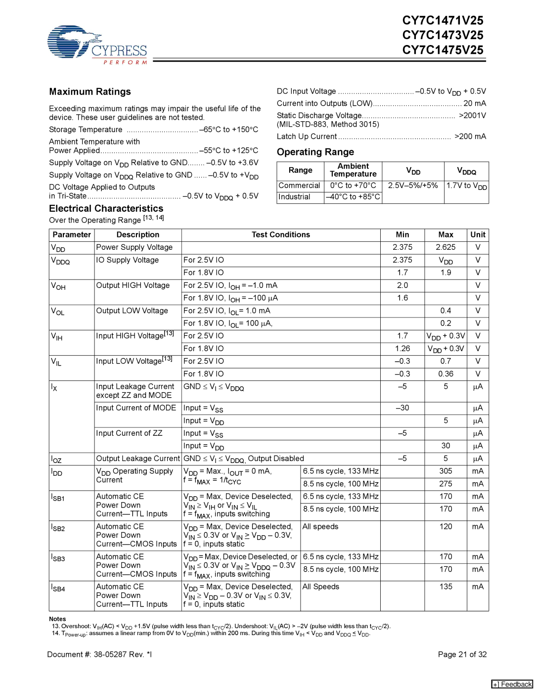
Maximum Ratings
Exceeding maximum ratings may impair the useful life of the device. These user guidelines are not tested.
Storage Temperature | ||
Ambient Temperature with |
|
|
Power Applied | ||
Supply Voltage on VDD Relative to GND | ||
Supply Voltage on VDDQ Relative to GND | ||
DC Voltage Applied to Outputs |
|
|
in | ||
Electrical Characteristics
Over the Operating Range [13, 14]
DC Input Voltage | |
Current into Outputs (LOW) | 20 mA |
Static Discharge Voltage | >2001V |
| |
Latch Up Current | >200 mA |
Operating Range
Range | Ambient | VDD | VDDQ |
Temperature | |||
Commercial | 0°C to +70°C | 1.7V to VDD | |
Industrial |
|
|
Parameter | Description | Test Conditions | Min | Max | Unit | |
|
|
|
|
|
|
|
VDD | Power Supply Voltage |
|
| 2.375 | 2.625 | V |
VDDQ | IO Supply Voltage | For 2.5V IO |
| 2.375 | VDD | V |
|
| For 1.8V IO |
| 1.7 | 1.9 | V |
|
|
|
|
|
|
|
VOH | Output HIGH Voltage | For 2.5V IO, IOH = |
| 2.0 |
| V |
|
| For 1.8V IO, IOH = |
| 1.6 |
| V |
VOL | Output LOW Voltage | For 2.5V IO, IOL= 1.0 mA |
|
| 0.4 | V |
|
| For 1.8V IO, IOL= 100 ∝A, |
|
| 0.2 | V |
VIH | Input HIGH Voltage[13] | For 2.5V IO |
| 1.7 | VDD + 0.3V | V |
|
| For 1.8V IO |
| 1.26 | VDD + 0.3V | V |
VIL | Input LOW Voltage[13] | For 2.5V IO |
| 0.7 | V | |
|
| For 1.8V IO |
| 0.36 | V | |
|
|
|
|
|
|
|
IX | Input Leakage Current | GND ≤ VI ≤ VDDQ |
| 5 | ∝A | |
| except ZZ and MODE |
|
|
|
|
|
| Input Current of MODE | Input = VSS |
|
| ∝A | |
|
| Input = VDD |
|
| 5 | ∝A |
| Input Current of ZZ | Input = VSS |
|
| ∝A | |
|
| Input = VDD |
|
| 30 | ∝A |
IOZ | Output Leakage Current | GND ≤ VI ≤ VDDQ, Output Disabled | 5 | ∝A | ||
IDD | VDD Operating Supply | VDD = Max., IOUT = 0 mA, | 6.5 ns cycle, 133 MHz |
| 305 | mA |
| Current | f = fMAX = 1/tCYC |
|
|
|
|
| 8.5 ns cycle, 100 MHz |
| 275 | mA | ||
ISB1 | Automatic CE | VDD = Max, Device Deselected, | 6.5 ns cycle, 133 MHz |
| 170 | mA |
| Power Down | VIN ≥ VIH or VIN ≤ VIL |
|
|
|
|
| 8.5 ns cycle, 100 MHz |
| 170 | mA | ||
| f = fMAX, inputs switching |
|
|
|
| |
ISB2 | Automatic CE | VDD = Max, Device Deselected, | All speeds |
| 120 | mA |
| Power Down | VIN ≤ 0.3V or VIN > VDD – 0.3V, |
|
|
|
|
| f = 0, inputs static |
|
|
|
| |
ISB3 | Automatic CE | VDD = Max, Device Deselected, or | 6.5 ns cycle, 133 MHz |
| 170 | mA |
| Power Down | VIN ≤ 0.3V or VIN > VDDQ – 0.3V |
|
|
|
|
| 8.5 ns cycle, 100 MHz |
| 170 | mA | ||
| f = fMAX, inputs switching |
|
|
|
| |
ISB4 | Automatic CE | VDD = Max, Device Deselected, | All Speeds |
| 135 | mA |
| Power Down | VIN ≥ VDD – 0.3V or VIN ≤ 0.3V, |
|
|
|
|
| f = 0, inputs static |
|
|
|
| |
Notes
13.Overshoot: VIH(AC) < VDD +1.5V (pulse width less than tCYC/2). Undershoot: VIL(AC) >
14.
Document #: | Page 21 of 32 |
[+] Feedback