CY7C1471V25
CY7C1473V25
CY7C1475V25
Document Title: CY7C1471V25/CY7C1473V25/CY7C1475V25,
Document Number:
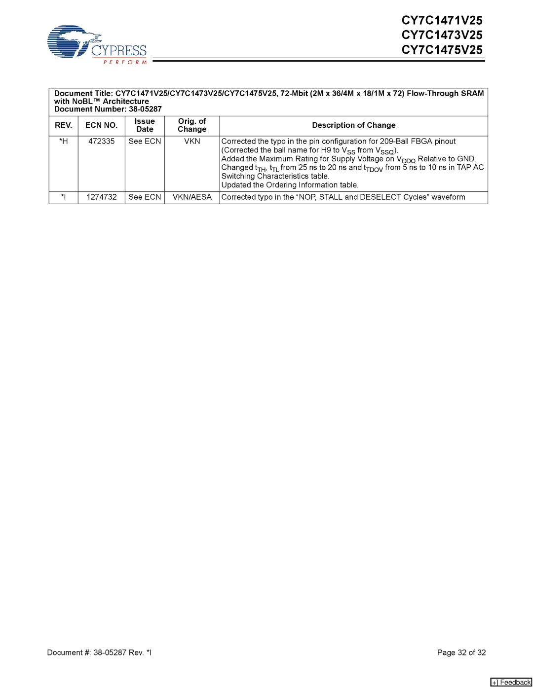
REV. | ECN NO. | Issue | Orig. of | Description of Change | |
Date | Change | ||||
|
|
| |||
|
|
|
|
| |
*H | 472335 | See ECN | VKN | Corrected the typo in the pin configuration for | |
|
|
|
| (Corrected the ball name for H9 to VSS from VSSQ). | |
|
|
|
| Added the Maximum Rating for Supply Voltage on VDDQ Relative to GND. | |
|
|
|
| Changed tTH, tTL from 25 ns to 20 ns and tTDOV from 5 ns to 10 ns in TAP AC | |
|
|
|
| Switching Characteristics table. | |
|
|
|
| Updated the Ordering Information table. | |
*I | 1274732 | See ECN | VKN/AESA | Corrected typo in the “NOP, STALL and DESELECT Cycles” waveform | |
|
|
|
|
|
Document #: | Page 32 of 32 |
[+] Feedback