CY7C1471V25
CY7C1473V25
CY7C1475V25
Switching Waveforms
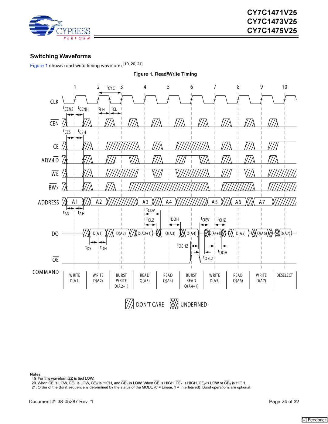
Figure 1 shows read-write timing waveform.[19, 20, 21]
|
|
| Figure 1. Read/Write Timing |
|
|
|
| ||
1 | 2 | tCYC 3 | 4 | 5 | 6 | 7 | 8 | 9 | 10 |
CLK |
|
|
|
|
|
|
|
|
|
tCENS tCENH | tCH | tCL |
|
|
|
|
|
|
|
CEN
tCES tCEH
CE ![]()
ADV/LD
W E
BW X
ADDRESS  A1
A1  A2
A2
| tAS tAH |
|
DQ |
| D(A1) |
| tDS | tDH |
OE |
|
|
COM M AND | W RITE | W RITE |
| ||
| D(A1) | D(A2) |
| A3 | A4 |
|
| A5 | A6 | A7 |
|
| tCDV |
|
|
|
|
|
|
|
| tCLZ | tDOH | tOEV | tCHZ |
|
|
| |
D(A2) | D(A2+1) | Q(A3) | Q(A4) |
| Q(A4+1) | D(A5) | Q(A6) | D(A7) |
|
|
| tOEHZ |
| tDOH |
|
|
|
|
|
|
|
|
|
|
| |
|
|
|
| tOELZ |
|
|
| |
BURST | READ | READ | BURST |
| W RITE | READ | W RITE | DESELECT |
W RITE | Q(A3) | Q(A4) | READ |
| D(A5) | Q(A6) | D(A7) |
|
D(A2+1) |
|
| Q(A4+1) |
|
|
|
|
|
DON’T CARE | UNDEFINED |
Notes
19.For this waveform ZZ is tied LOW.
20.When CE is LOW, CE1 is LOW, CE2 is HIGH, and CE3 is LOW. When CE is HIGH, CE1 is HIGH, CE2 is LOW or CE3 is HIGH.
21.Order of the Burst sequence is determined by the status of the MODE (0 = Linear, 1 = Interleaved). Burst operations are optional.
Document #: | Page 24 of 32 |
[+] Feedback