CY7C1471V25
CY7C1473V25
CY7C1475V25
Because the CY7C1471V25, CY7C1473V25, and CY7C1475V25 are common IO devices, data must not be driven into the device while the outputs are active. The OE can be deasserted HIGH before presenting data to the DQs and DQPX inputs. This
Burst Write Accesses
The CY7C1471V25, CY7C1473V25, and CY7C1475V25 have an
Sleep Mode
The ZZ input pin is an asynchronous input. Asserting ZZ places the SRAM in a power conservation “sleep” mode. Two clock cycles are required to enter into or exit from this “sleep” mode. While in this mode, data integrity is guaranteed. Accesses pending when entering the “sleep” mode are not considered valid nor is the completion of the operation guaranteed. The device must be deselected before entering the “sleep” mode. CE1, CE2, and CE3, must remain inactive for the duration of tZZREC after the ZZ input returns LOW.
Interleaved Burst Address Table (MODE = Floating or VDD)
First | Second | Third | Fourth |
Address | Address | Address | Address |
A1: A0 | A1: A0 | A1: A0 | A1: A0 |
00 | 01 | 10 | 11 |
|
|
|
|
01 | 00 | 11 | 10 |
|
|
|
|
10 | 11 | 00 | 01 |
|
|
|
|
11 | 10 | 01 | 00 |
|
|
|
|
Linear Burst Address Table (MODE = GND)
First | Second | Third | Fourth |
Address | Address | Address | Address |
A1: A0 | A1: A0 | A1: A0 | A1: A0 |
00 | 01 | 10 | 11 |
|
|
|
|
01 | 10 | 11 | 00 |
|
|
|
|
10 | 11 | 00 | 01 |
|
|
|
|
11 | 00 | 01 | 10 |
|
|
|
|
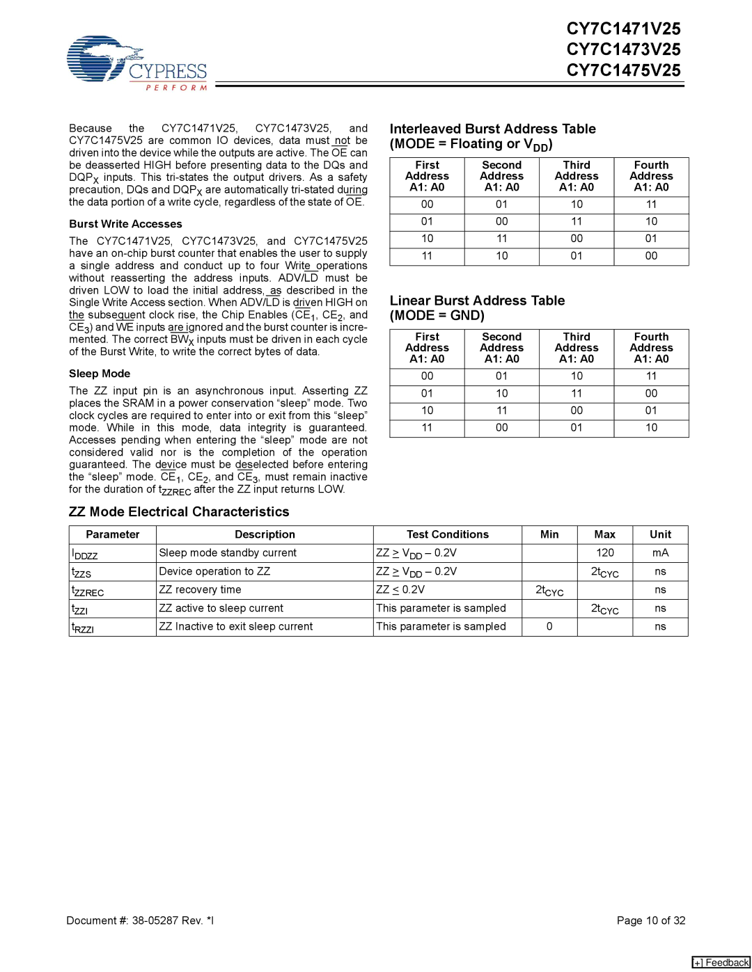
ZZ Mode Electrical Characteristics
Parameter | Description | Test Conditions | Min | Max | Unit |
|
|
|
|
|
|
IDDZZ | Sleep mode standby current | ZZ > VDD – 0.2V |
| 120 | mA |
tZZS | Device operation to ZZ | ZZ > VDD – 0.2V |
| 2tCYC | ns |
tZZREC | ZZ recovery time | ZZ < 0.2V | 2tCYC |
| ns |
tZZI | ZZ active to sleep current | This parameter is sampled |
| 2tCYC | ns |
tRZZI | ZZ Inactive to exit sleep current | This parameter is sampled | 0 |
| ns |
Document #: | Page 10 of 32 |
[+] Feedback