CY62136EV30
MoBL®
Thermal Resistance[8]
Parameter | Description | Test Conditions | VFBGA | TSOP II | Unit |
Package | Package | ||||
|
|
|
|
|
|
ΘJA | Thermal Resistance | Still Air, soldered on a 3 × 4.5 inch, | 75 | 77 | °C/W |
| (Junction to Ambient)[8] | printed circuit board |
|
|
|
ΘJC | Thermal Resistance |
| 10 | 13 | °C/W |
| (Junction to Case)[8] |
|
|
|
|
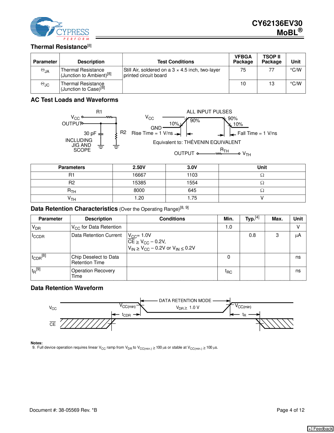
AC Test Loads and Waveforms
R1
VCC ![]()
OUTPUT![]()
30 pF ![]()
INCLUDING
JIG AND
SCOPE
| VCC |
|
|
|
|
|
|
|
| ALL INPUT PULSES |
| |||||||||||
|
|
|
|
|
|
|
|
|
|
|
|
|
|
|
| 90% |
|
| ||||
|
|
| 10% |
|
|
|
|
|
| 90% |
|
|
|
|
|
|
| 10% | ||||
R2 | GND |
|
|
|
|
|
|
|
|
|
|
|
|
|
|
|
| |||||
|
|
|
|
|
|
|
|
|
|
|
|
|
|
|
|
|
|
|
| |||
|
|
|
|
|
|
|
|
|
|
|
|
|
|
|
|
|
|
|
| |||
Rise Time = 1 | V/ns |
|
|
|
|
|
|
|
|
|
|
|
|
|
|
| Fall Time = 1 V/ns | |||||
| Equivalent to: THÉVENIN EQUIVALENT |
| ||||||||||||||||||||
|
|
| OUTPUT |
| RTH | VTH | ||||||||||||||||
|
|
|
|
|
|
|
|
|
|
|
|
| ||||||||||
Parameters | 2.50V | 3.0V | Unit |
R1 | 16667 | 1103 | Ω |
|
|
|
|
R2 | 15385 | 1554 | Ω |
|
|
|
|
RTH | 8000 | 645 | Ω |
VTH | 1.20 | 1.75 | V |
Data Retention Characteristics (Over the Operating Range)[8, 9]
Parameter | Description | Conditions | Min. | Typ.[4] | Max. | Unit |
VDR | VCC for Data Retention |
| 1.0 |
|
| V |
ICCDR | Data Retention Current | VCC= 1.0V |
| 0.8 | 3 | ∝A |
|
| CE > VCC – 0.2V, |
|
|
|
|
|
| VIN > VCC – 0.2V or VIN < 0.2V |
|
|
|
|
tCDR[8] | Chip Deselect to Data |
| 0 |
|
| ns |
| Retention Time |
|
|
|
|
|
t [9] | Operation Recovery |
| t |
|
| ns |
R | Time |
| RC |
|
|
|
|
|
|
|
|
| |
|
|
|
|
|
|
|
Data Retention Waveform
| VCC(min) | DATA RETENTION MODE | VCC(min) |
VCC | VDR > 1.0 V | ||
| tCDR |
| tR |
CE |
|
|
|
Notes:
9. Full device operation requires linear VCC ramp from VDR to VCC(min.) > 100 ∝s or stable at VCC(min.) > 100 ∝s.
Document #: | Page 4 of 12 |
[+] Feedback