
CY62138CV25, CY62138CV30, CY62138FV30, CY62138CV33 specifications
The Cypress CY62138 series, which includes the CY62138CV30, CY62138CV33, CY62138CV25, and CY62138FV30, represents a family of high-performance CMOS Static Random Access Memory (SRAM) devices. These components are widely utilized in various applications due to their speed, density, and reliability.One of the key features of the CY62138 series is its memory density. These SRAMs provide 2Megwords x 8Bit (2M x 8) configurations, making them suitable for applications that require substantial memory capacity without the complexities associated with dynamic RAM technologies. The components are built using advanced CMOS technology, which enables low power consumption while maintaining high-speed performance.
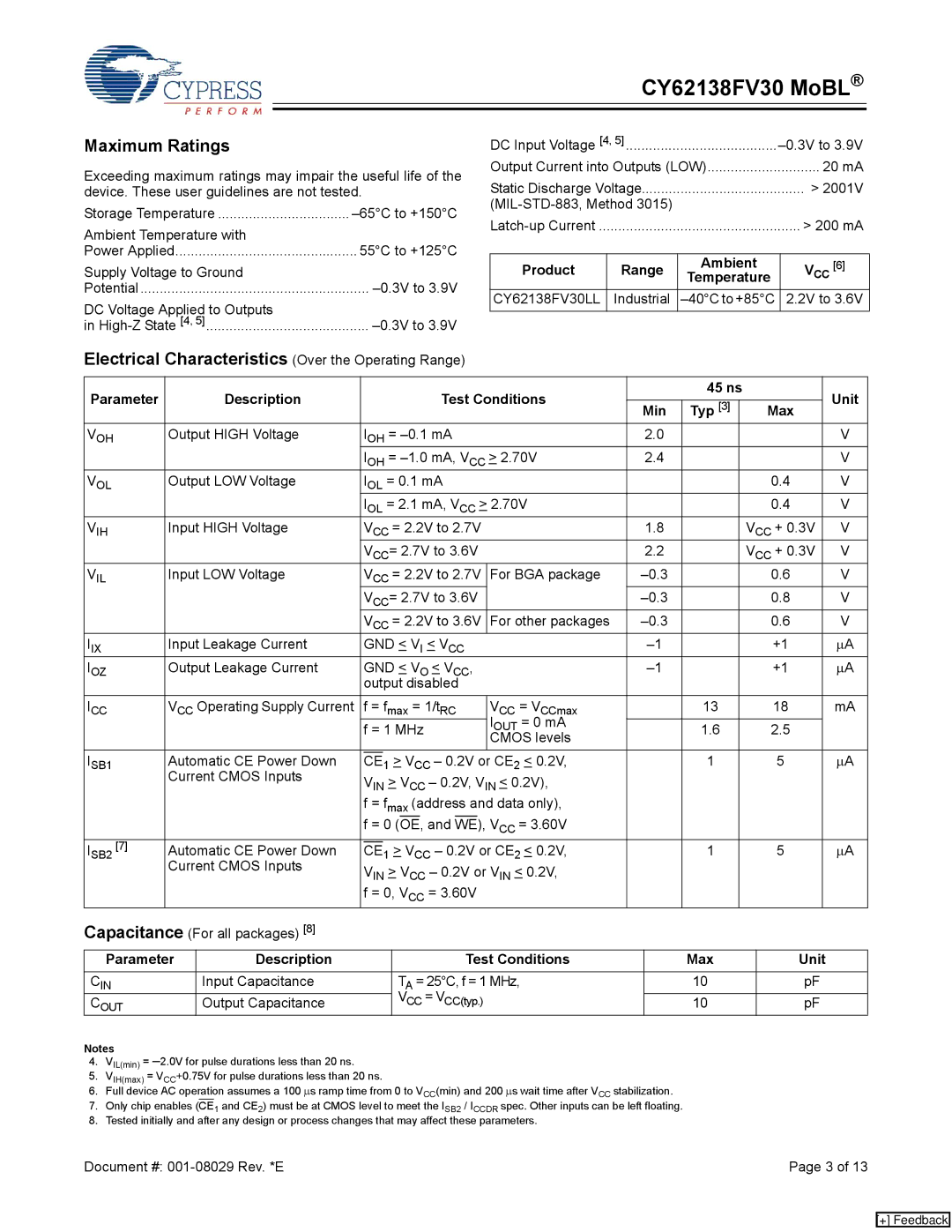
The devices in this series operate under a voltage range of 2.7V to 3.6V for the CY62138CV models and can operate at clock speeds of 30ns, 33ns, and 25ns, depending on the specific variant. The CY62138FV30 variant, optimized for fast operation, can achieve access times as low as 30ns. This speed is particularly advantageous in applications such as buffering, caching, and other scenarios where rapid data access is critical.
Another prominent feature is the CY62138 series' support for a straightforward interface, which simplifies design integration. The SRAMs boast a asynchronous operation that eliminates the need for complex timing requirements, thereby easing the design process for engineers. The devices support both byte and word access modes, providing flexibility in handling data.
In terms of reliability, the CY62138 SRAMs are designed to operate over an extensive temperature range, making them suitable for harsh environments. They also feature a write protection mechanism, ensuring that data integrity is maintained during unexpected power fluctuations.
In summary, the Cypress CY62138 series combines high density, rapid access times, low power consumption, and robust reliability features, making it a highly effective choice for a wide range of applications, including telecommunications, industrial control systems, and consumer electronics. As technology evolves, devices from this series continue to meet the demands for reliable, high-speed memory solutions in various sectors.