CY7C1354C
CY7C1356C
3.3V TAP AC Test Conditions
Input pulse levels | VSS to 3.3V |
Input rise and fall times | 1 ns |
Input timing reference levels | 1.5V |
Output reference levels | 1.5V |
Test load termination supply voltage | 1.5V |
2.5V TAP AC Test Conditions
Input pulse levels | VSS to 2.5V |
Input rise and fall time | 1 ns |
Input timing reference levels | 1.25V |
Output reference levels | 1.25V |
Test load termination supply voltage | 1.25V |
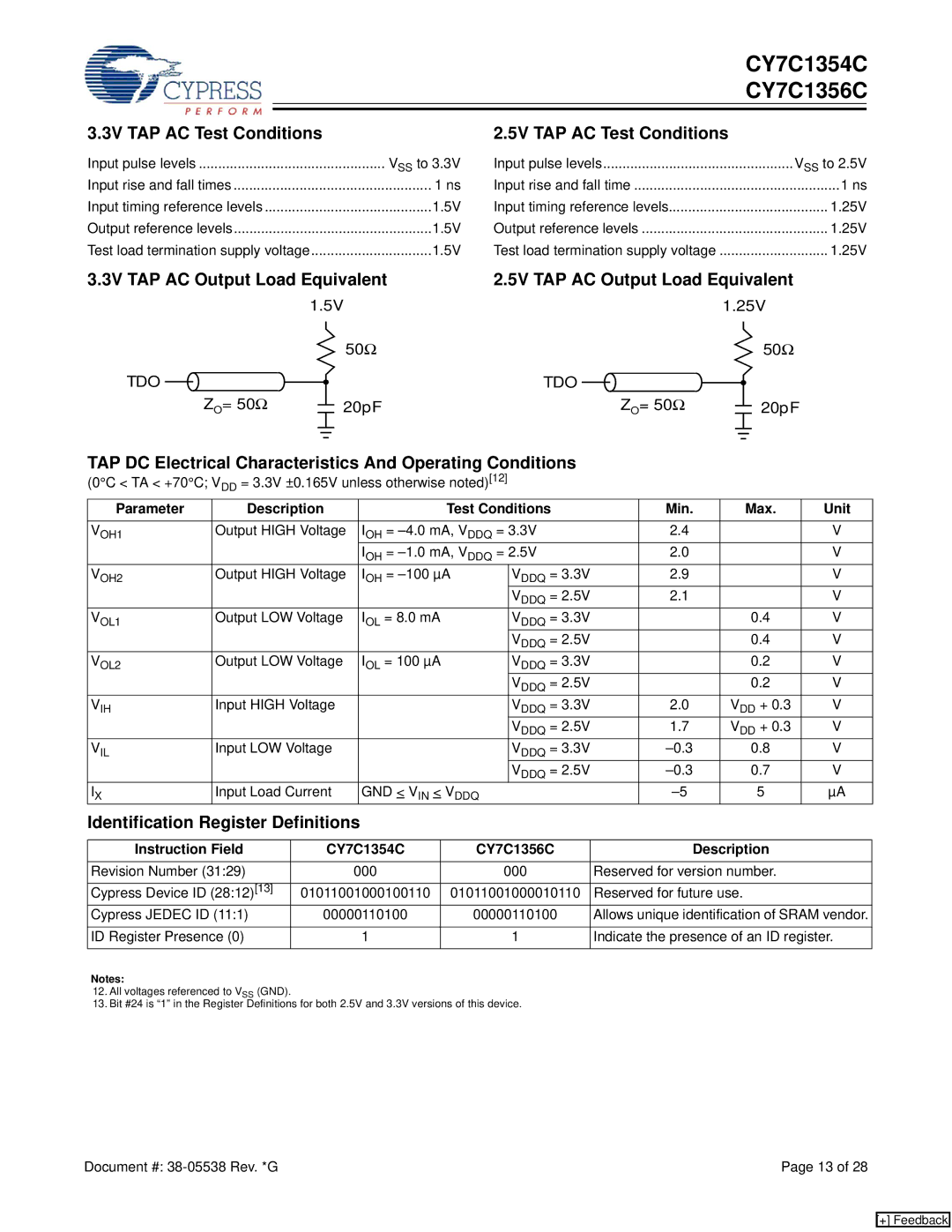
3.3V TAP AC Output Load Equivalent | 2.5V TAP AC Output Load Equivalent |
| ||||||||||||||||||||||||||||||
|
|
|
|
|
| 1.5V |
|
|
|
|
|
|
|
|
| 1.25V |
| |||||||||||||||
|
|
|
|
|
|
|
|
|
|
|
|
|
| 50Ω |
|
|
|
|
|
|
|
|
|
|
|
|
|
|
| 50Ω |
| |
TDO |
|
|
|
|
|
|
|
|
|
|
|
|
|
|
|
| TDO |
|
|
|
|
|
|
|
|
|
|
|
|
|
|
|
|
|
|
|
|
|
|
|
|
|
|
|
|
|
|
|
|
|
|
|
|
|
|
|
|
|
|
|
| ||||
|
|
|
|
|
|
|
|
|
|
|
|
|
|
|
|
|
|
|
|
|
|
|
|
|
|
|
|
|
| |||
|
|
| ZO= 50Ω |
|
|
|
|
| 20pF |
|
|
|
| ZO= 50Ω |
|
|
|
|
|
|
|
| 20pF |
| ||||||||
|
|
|
|
|
|
|
|
|
|
|
|
|
|
|
|
|
|
|
|
|
|
| ||||||||||
|
|
|
|
|
|
|
|
|
|
|
|
|
|
|
|
|
|
|
|
|
|
|
|
|
|
|
| |||||
|
|
|
|
|
|
|
|
|
|
|
|
|
|
|
|
|
|
|
|
|
|
|
|
|
|
|
|
|
|
|
|
|
|
|
|
|
|
|
|
|
|
|
|
|
|
|
|
|
|
|
|
|
|
|
| ||||||||||
TAP DC Electrical Characteristics And Operating Conditions |
|
|
|
|
|
|
|
|
|
|
|
|
|
| ||||||||||||||||||
(0°C < TA < +70°C; V = 3.3V ±0.165V unless otherwise noted)[12] |
|
|
|
|
|
|
|
|
|
|
|
|
|
| ||||||||||||||||||
|
|
|
| DD |
|
|
|
|
|
|
|
|
|
|
|
|
|
|
|
|
|
|
| |||||||||
Parameter |
|
| Description |
| Test Conditions |
|
| Min. |
|
|
|
|
| Max. | Unit | |||||||||||||||||
VOH1 |
|
| Output HIGH Voltage | IOH = |
|
| 2.4 |
|
|
|
|
|
|
|
|
|
| V | ||||||||||||||
|
|
|
|
|
|
|
|
|
|
|
|
|
|
| IOH = |
|
| 2.0 |
|
|
|
|
|
|
|
|
|
| V | |||
VOH2 |
|
| Output HIGH Voltage | IOH = |
| VDDQ = 3.3V |
|
| 2.9 |
|
|
|
|
|
|
|
|
|
| V | ||||||||||||
|
|
|
|
|
|
|
|
|
|
|
|
|
|
|
|
| VDDQ = 2.5V |
|
| 2.1 |
|
|
|
|
|
|
|
|
|
| V | |
VOL1 |
|
| Output LOW Voltage |
| IOL = 8.0 mA |
| VDDQ = 3.3V |
|
|
|
|
| 0.4 | V | ||||||||||||||||||
|
|
|
|
|
|
|
|
|
|
|
|
|
|
|
|
| VDDQ = 2.5V |
|
|
|
|
| 0.4 | V | ||||||||
VOL2 |
|
| Output LOW Voltage |
| IOL = 100 µA |
| VDDQ = 3.3V |
|
|
|
|
| 0.2 | V | ||||||||||||||||||
|
|
|
|
|
|
|
|
|
|
|
|
|
|
|
|
| VDDQ = 2.5V |
|
|
|
|
| 0.2 | V | ||||||||
VIH |
|
| Input HIGH Voltage |
|
|
| VDDQ = 3.3V |
|
| 2.0 |
|
| VDD + 0.3 | V | ||||||||||||||||||
|
|
|
|
|
|
|
|
|
|
|
|
|
|
|
|
| VDDQ = 2.5V |
|
| 1.7 |
|
| VDD + 0.3 | V | ||||||||
VIL |
|
| Input LOW Voltage |
|
|
| VDDQ = 3.3V |
|
|
| 0.8 | V | ||||||||||||||||||||
|
|
|
|
|
|
|
|
|
|
|
|
|
|
|
|
| VDDQ = 2.5V |
|
|
| 0.7 | V | ||||||||||
IX |
|
| Input Load Current |
| GND < VIN < VDDQ |
|
|
|
|
|
| 5 | µA | |||||||||||||||||||
Identification Register Definitions
Instruction Field | CY7C1354C | CY7C1356C | Description |
Revision Number (31:29) | 000 | 000 | Reserved for version number. |
|
|
|
|
Cypress Device ID (28:12)[13] | 01011001000100110 | 01011001000010110 | Reserved for future use. |
Cypress JEDEC ID (11:1) | 00000110100 | 00000110100 | Allows unique identification of SRAM vendor. |
|
|
|
|
ID Register Presence (0) | 1 | 1 | Indicate the presence of an ID register. |
|
|
|
|
Notes:
12.All voltages referenced to VSS (GND).
13.Bit #24 is “1” in the Register Definitions for both 2.5V and 3.3V versions of this device.
Document #: | Page 13 of 28 |
[+] Feedback