|
|
|
|
|
|
|
|
|
|
|
|
|
|
|
|
| CY7C1354C | ||||
|
|
|
|
|
|
|
|
|
|
|
|
|
|
|
|
| CY7C1356C | ||||
|
|
|
|
|
|
|
|
|
|
|
|
|
| ||||||||
|
|
|
|
|
|
|
|
|
|
|
|
|
|
|
|
|
|
|
|
|
|
|
|
|
|
|
|
|
|
|
|
|
|
|
|
|
|
|
|
|
|
|
|
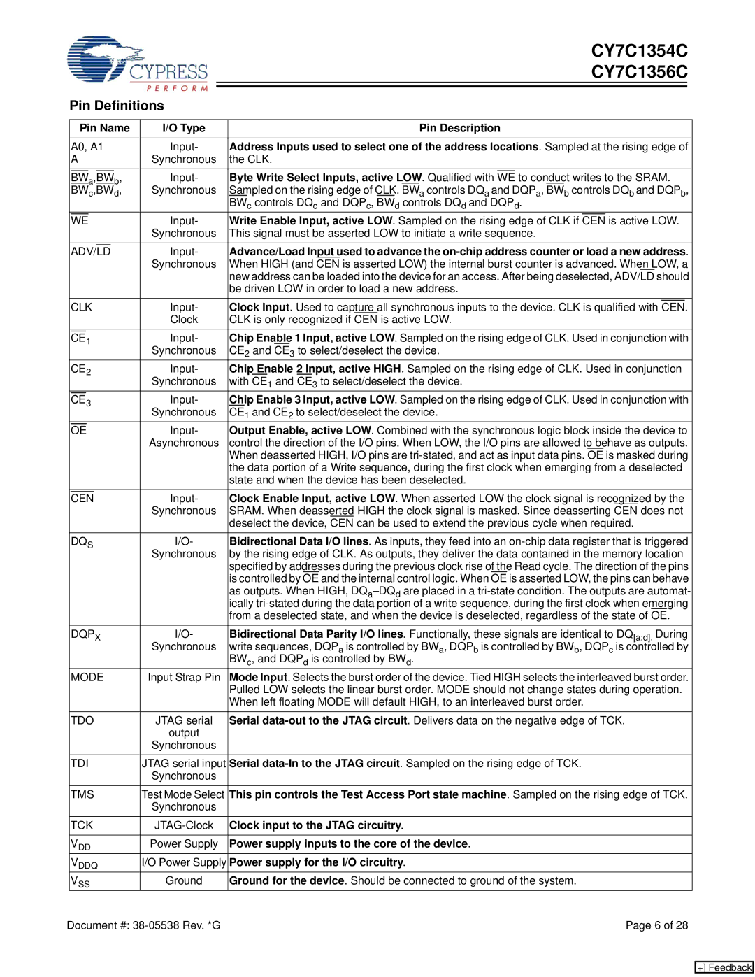
| Pin Definitions |
|
|
|
|
|
|
|
| ||||||||||||
|
|
|
| ||||||||||||||||||
| Pin Name | I/O Type | Pin Description | ||||||||||||||||||
|
|
|
| ||||||||||||||||||
| A0, A1 | Input- | Address Inputs used to select one of the address locations. Sampled at the rising edge of | ||||||||||||||||||
| A | Synchronous | the CLK. | ||||||||||||||||||
|
|
|
| a, |
|
|
| b, | Input- | Byte Write Select Inputs, active LOW. Qualified with |
| to conduct writes to the SRAM. | |||||||||
| BW | BW | WE | ||||||||||||||||||
| BWc,BWd, | Synchronous | Sampled on the rising edge of CLK. BWa controls DQa and DQPa, BWb controls DQb and DQPb, | ||||||||||||||||||
|
|
|
|
|
|
|
|
|
|
|
|
|
| BWc controls DQc and DQPc, BWd controls DQd and DQPd. | |||||||
|
|
|
|
|
|
|
|
| Input- | Write Enable Input, active LOW. Sampled on the rising edge of CLK if |
| is active LOW. | |||||||||
| WE | CEN | |||||||||||||||||||
|
|
|
|
|
|
|
|
|
|
| Synchronous | This signal must be asserted LOW to initiate a write sequence. | |||||||||
|
|
|
|
|
|
|
|
|
|
| Input- | Advance/Load Input used to advance the | |||||||||
| ADV/LD |
| |||||||||||||||||||
|
|
|
|
|
|
|
|
|
|
| Synchronous | When HIGH (and CEN is asserted LOW) the internal burst counter is advanced. When LOW, a | |||||||||
|
|
|
|
|
|
|
|
|
|
|
|
|
| new address can be loaded into the device for an access. After being deselected, ADV/LD should | |||||||
|
|
|
|
|
|
|
|
|
|
|
|
|
| be driven LOW in order to load a new address. | |||||||
| CLK | Input- | Clock Input. Used to capture all synchronous inputs to the device. CLK is qualified with |
|
| ||||||||||||||||
| CEN. | ||||||||||||||||||||
|
|
|
|
|
|
|
|
|
|
| Clock | CLK is only recognized if CEN is active LOW. | |||||||||
|
| 1 |
| Input- | Chip Enable 1 Input, active LOW. Sampled on the rising edge of CLK. Used in conjunction with | ||||||||||||||||
| CE | ||||||||||||||||||||
|
|
|
|
|
|
|
|
|
|
| Synchronous | CE2 and CE3 to select/deselect the device. | |||||||||
| CE2 | Input- | Chip Enable 2 Input, active HIGH. Sampled on the rising edge of CLK. Used in conjunction | ||||||||||||||||||
|
|
|
|
|
|
|
|
|
|
| Synchronous | with CE1 and CE3 to select/deselect the device. | |||||||||
|
| 3 |
| Input- | Chip Enable 3 Input, active LOW. Sampled on the rising edge of CLK. Used in conjunction with | ||||||||||||||||
| CE | ||||||||||||||||||||
|
|
|
|
|
|
|
|
|
|
| Synchronous | CE1 and CE2 to select/deselect the device. | |||||||||
|
|
|
|
| Input- | Output Enable, active LOW. Combined with the synchronous logic block inside the device to | |||||||||||||||
| OE | ||||||||||||||||||||
|
|
|
|
|
|
|
|
|
|
| Asynchronous | control the direction of the I/O pins. When LOW, the I/O pins are allowed to behave as outputs. | |||||||||
|
|
|
|
|
|
|
|
|
|
|
|
|
| When deasserted HIGH, I/O pins are | |||||||
|
|
|
|
|
|
|
|
|
|
|
|
|
| the data portion of a Write sequence, during the first clock when emerging from a deselected | |||||||
|
|
|
|
|
|
|
|
|
|
|
|
|
| state and when the device has been deselected. | |||||||
|
|
|
|
|
|
| Input- | Clock Enable Input, active LOW. When asserted LOW the clock signal is recognized by the | |||||||||||||
| CEN | ||||||||||||||||||||
|
|
|
|
|
|
|
|
|
|
| Synchronous | SRAM. When deasserted HIGH the clock signal is masked. Since deasserting CEN does not | |||||||||
|
|
|
|
|
|
|
|
|
|
|
|
|
| deselect the device, CEN can be used to extend the previous cycle when required. | |||||||
| DQS | I/O- | Bidirectional Data I/O lines. As inputs, they feed into an | ||||||||||||||||||
|
|
|
|
|
|
|
|
|
|
| Synchronous | by the rising edge of CLK. As outputs, they deliver the data contained in the memory location | |||||||||
|
|
|
|
|
|
|
|
|
|
|
|
|
| specified by addresses during the previous clock rise of the Read cycle. The direction of the pins | |||||||
|
|
|
|
|
|
|
|
|
|
|
|
|
| is controlled by OE and the internal control logic. When OE is asserted LOW, the pins can behave | |||||||
|
|
|
|
|
|
|
|
|
|
|
|
|
| as outputs. When HIGH, | |||||||
|
|
|
|
|
|
|
|
|
|
|
|
|
| ically | |||||||
|
|
|
|
|
|
|
|
|
|
|
|
|
| from a deselected state, and when the device is deselected, regardless of the state of OE. | |||||||
| DQPX | I/O- | Bidirectional Data Parity I/O lines. Functionally, these signals are identical to DQ[a:d]. During | ||||||||||||||||||
|
|
|
|
|
|
|
|
|
|
| Synchronous | write sequences, DQPa is controlled by BWa, DQPb is controlled by BWb, DQPc is controlled by | |||||||||
|
|
|
|
|
|
|
|
|
|
|
|
|
| BWc, and DQPd is controlled by BWd. | |||||||
| MODE | Input Strap Pin | Mode Input. Selects the burst order of the device. Tied HIGH selects the interleaved burst order. | ||||||||||||||||||
|
|
|
|
|
|
|
|
|
|
|
|
|
| Pulled LOW selects the linear burst order. MODE should not change states during operation. | |||||||
|
|
|
|
|
|
|
|
|
|
|
|
|
| When left floating MODE will default HIGH, to an interleaved burst order. | |||||||
| TDO | JTAG serial | Serial | ||||||||||||||||||
|
|
|
|
|
|
|
|
|
|
| output |
|
|
|
|
|
|
|
| ||
|
|
|
|
|
|
|
|
|
|
| Synchronous |
|
|
|
|
|
|
|
| ||
| TDI | JTAG serial input | Serial | ||||||||||||||||||
|
|
|
|
|
|
|
|
|
|
| Synchronous |
|
|
|
|
|
|
|
| ||
| TMS | Test Mode Select | This pin controls the Test Access Port state machine. Sampled on the rising edge of TCK. | ||||||||||||||||||
|
|
|
|
|
|
|
|
|
|
| Synchronous |
|
|
|
|
|
|
|
| ||
| TCK | Clock input to the JTAG circuitry. | |||||||||||||||||||
|
|
|
| ||||||||||||||||||
| VDD | Power Supply | Power supply inputs to the core of the device. | ||||||||||||||||||
| VDDQ | I/O Power Supply | Power supply for the I/O circuitry. | ||||||||||||||||||
| VSS | Ground | Ground for the device. Should be connected to ground of the system. | ||||||||||||||||||
Document #: |
|
|
|
| Page 6 of 28 | ||||||||||||||||
[+] Feedback