CY62146EV30 MoBL®
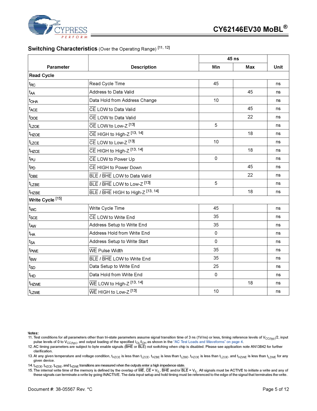
Switching Characteristics (Over the Operating Range) [11, 12]
|
|
|
|
|
|
|
|
|
| 45 ns |
| |
|
|
|
|
|
|
|
|
|
|
|
|
|
Parameter |
|
|
|
|
|
|
| Description | Min |
| Max | Unit |
|
|
|
|
|
|
|
|
|
|
|
|
|
Read Cycle |
|
|
|
|
|
|
|
|
|
|
| |
|
|
|
|
|
| |||||||
tRC |
| Read Cycle Time | 45 |
|
| ns | ||||||
tAA |
| Address to Data Valid |
|
| 45 | ns | ||||||
tOHA |
| Data Hold from Address Change | 10 |
|
| ns | ||||||
tACE |
|
|
|
| LOW to Data Valid |
|
| 45 | ns | |||
CE |
| |||||||||||
tDOE |
|
|
|
| LOW to Data Valid |
|
| 22 | ns | |||
OE |
| |||||||||||
tLZOE |
|
|
|
| LOW to | 5 |
|
| ns | |||
OE |
|
| ||||||||||
tHZOE |
|
|
|
| HIGH to |
|
| 18 | ns | |||
OE |
| |||||||||||
tLZCE |
|
|
| LOW to | 10 |
|
| ns | ||||
CE |
|
| ||||||||||
tHZCE |
|
|
| HIGH to |
|
| 18 | ns | ||||
CE |
| |||||||||||
tPU |
|
|
| LOW to Power Up | 0 |
|
| ns | ||||
CE |
|
| ||||||||||
tPD |
|
|
| HIGH to Power Down |
|
| 45 | ns | ||||
CE |
| |||||||||||
tDBE |
|
|
|
|
| / |
| LOW to Data Valid |
|
| 22 | ns |
BLE | BHE |
| ||||||||||
tLZBE |
|
|
|
|
| / |
| LOW to | 5 |
|
| ns |
BLE | BHE |
|
| |||||||||
tHZBE |
|
|
|
|
| / |
| HIGH to |
|
| 18 | ns |
BLE | BHE |
| ||||||||||
Write Cycle [15] |
|
|
|
|
|
|
|
|
|
|
|
|
tWC |
| Write Cycle Time | 45 |
|
| ns | ||||||
tSCE |
|
|
| LOW to Write End | 35 |
|
| ns | ||||
CE |
|
| ||||||||||
tAW |
| Address Setup to Write End | 35 |
|
| ns | ||||||
tHA |
| Address Hold from Write End | 0 |
|
| ns | ||||||
tSA |
| Address Setup to Write Start | 0 |
|
| ns | ||||||
tPWE |
|
|
|
| Pulse Width | 35 |
|
| ns | |||
WE |
|
| ||||||||||
tBW |
|
|
|
|
| / |
| LOW to Write End | 35 |
|
| ns |
BLE | BHE |
|
| |||||||||
tSD |
| Data Setup to Write End | 25 |
|
| ns | ||||||
tHD |
| Data Hold from Write End | 0 |
|
| ns | ||||||
tHZWE |
|
|
|
| LOW to |
|
| 18 | ns | |||
WE |
| |||||||||||
tLZWE |
|
|
|
| HIGH to | 10 |
|
| ns | |||
WE |
|
| ||||||||||
Notes:
11.Test conditions for all parameters other than
12.AC timing parameters are subject to byte enable signals (BHE or BLE) not switching when chip is disabled. Please see application note AN13842 for further clarification.
13.At any given temperature and voltage condition, tHZCE is less than tLZCE, tHZBE is less than tLZBE, tHZOE is less than tLZOE, and tHZWE is less than tLZWE for any given device.
14.tHZOE, tHZCE, tHZBE, and tHZWE transitions are measured when the outputs enter a high impedence state.
15.The internal write time of the memory is defined by the overlap of WE, CE = VIL, BHE and/or BLE = VIL. All signals must be ACTIVE to initiate a write and any of these signals can terminate a write by going INACTIVE. The data input setup and hold timing must be referenced to the edge of the signal that terminates the write.
Document #: | Page 5 of 12 |