
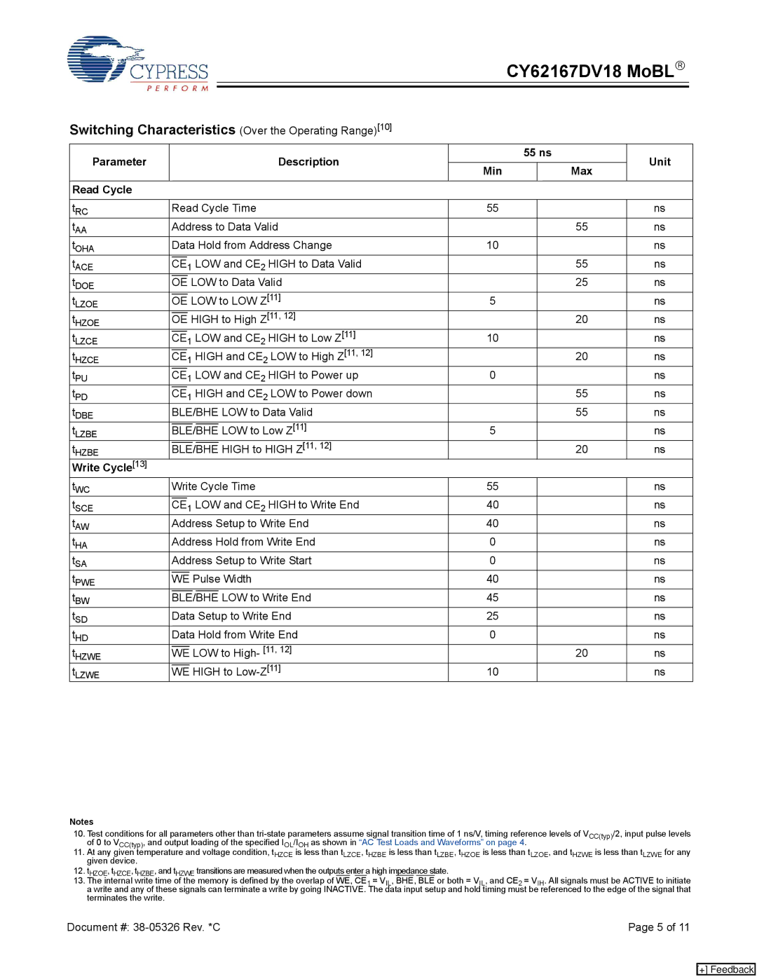
CY62167DV18 specifications
The Cypress CY62167DV18 is a high-performance, low-power static RAM (SRAM) device designed for a variety of applications where speed and efficiency are critical. This memory chip is especially notable for its compact footprint and advanced features, making it ideal for use in portable electronics, consumer products, telecommunications, and networking equipment.One of the main features of the CY62167DV18 is its access time of 10 nanoseconds, allowing for rapid data retrieval and processing. With a data width of 16 bits, the device provides significant data bandwidth, which is essential for modern applications requiring fast processing capabilities. It operates on a power supply voltage of 1.8V, thereby ensuring low power consumption, which is a crucial factor in battery-operated devices.
The CY62167DV18 employs Cypress’s advanced SRAM technology, which improves speed while reducing latency. This SRAM is fabricated using a highly reliable process technology that enhances durability and performance. Additionally, the chip's static nature eliminates the need for refresh cycles, contributing to quick access times and more straightforward system designs compared to dynamic RAM (DRAM).
Another characteristic of the CY62167DV18 is its compatibility with various memory bus standards, including the popular 32-bit asynchronous interface. This adaptability allows the chip to easily integrate into existing designs without requiring major modifications. Furthermore, the device supports a wide temperature range, making it suitable for both consumer and industrial applications.
The CY62167DV18 comes with built-in features such as a chip enable input (CE), write enable input (WE), and output enable input (OE). These functionalities streamline control and management of memory access, enabling engineers to design efficient and reliable systems. The chip is available in a compact 48-ball BGA (Ball Grid Array) package, which saves space on printed circuit boards and enhances thermal performance.
In summary, the Cypress CY62167DV18 is a robust, high-speed SRAM solution that combines advanced technology with low power consumption. Its impressive access times, low-voltage operation, compatibility with multiple standards, and compact design make it a versatile choice for a broad range of applications, from consumer electronics to sophisticated industrial systems. As the demand for faster and more efficient memory solutions continues to grow, the CY62167DV18 stands out as a reliable option for developers seeking to enhance their product performance.