CY7C024AV/024BV/025AV/026AV
CY7C0241AV/0251AV/036AV
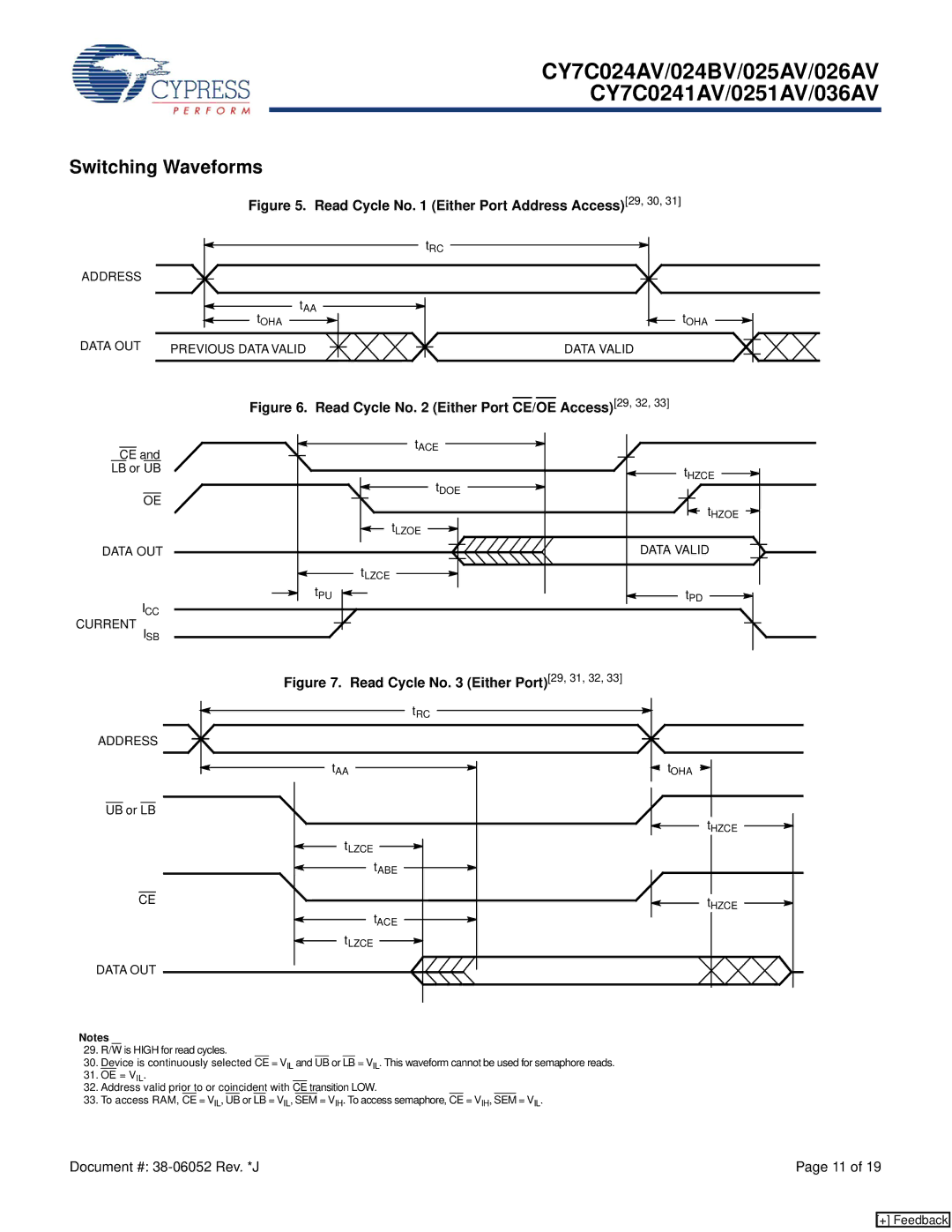
Switching Waveforms
Figure 5. Read Cycle No. 1 (Either Port Address Access)[29, 30, 31]
|
| tRC |
ADDRESS |
|
|
| tAA | tOHA |
| tOHA | |
DATA OUT | PREVIOUS DATA VALID | DATA VALID |
CE and
LB or UB
OE
DATA OUT
ICC
CURRENT
ISB
Figure 6. Read Cycle No. 2 (Either Port CE/OE Access)[29, 32, 33]
| tACE |
| tHZCE |
| tDOE |
| tHZOE |
| tLZOE |
| DATA VALID |
| tLZCE |
tPU | t |
| PD |
Figure 7. Read Cycle No. 3 (Either Port)[29, 31, 32, 33]
tRC
ADDRESS
tAA
UB or LB
tLZCE
tABE
CE
tACE
tLZCE
DATA OUT
tOHA
tHZCE |
tHZCE |
Notes
29.R/W is HIGH for read cycles.
30.Device is continuously selected CE = VIL and UB or LB = VIL. This waveform cannot be used for semaphore reads.
31.OE = VIL.
32.Address valid prior to or coincident with CE transition LOW.
33.To access RAM, CE = VIL, UB or LB = VIL, SEM = VIH. To access semaphore, CE = VIH, SEM = VIL.
Document #: | Page 11 of 19 |
[+] Feedback