CY7C024AV/024BV/025AV/026AV
CY7C0241AV/0251AV/036AV
3.3V 4K/8K/16K x 16/18 Dual-Port Static RAM
Features
■True
■4, 8 or 16K × 16 organization
■(CY7C024AV/024BV [1]/ 025AV/026AV)
■4 or 8K × 18 organization (CY7C0241AV/0251AV)
■16K × 18 organization (CY7C036AV)
■0.35 micron CMOS for optimum speed and power
■High speed access: 20 and 25 ns
■Low operating power
❐Active: ICC = 115 mA (typical)
❐Standby: ISB3 = 10 μA (typical)
■Fully asynchronous operation
■Automatic power down
■Expandable data bus to 32 bits, 36 bits or more using Master and Slave chip select when using more than one device
■On chip arbitration logic
■Semaphores included to permit software handshaking between ports
■INT flag for
■Separate upper byte and lower byte control
■Pin select for Master or Slave (M/S)
■Commercial and industrial temperature ranges
■Available in
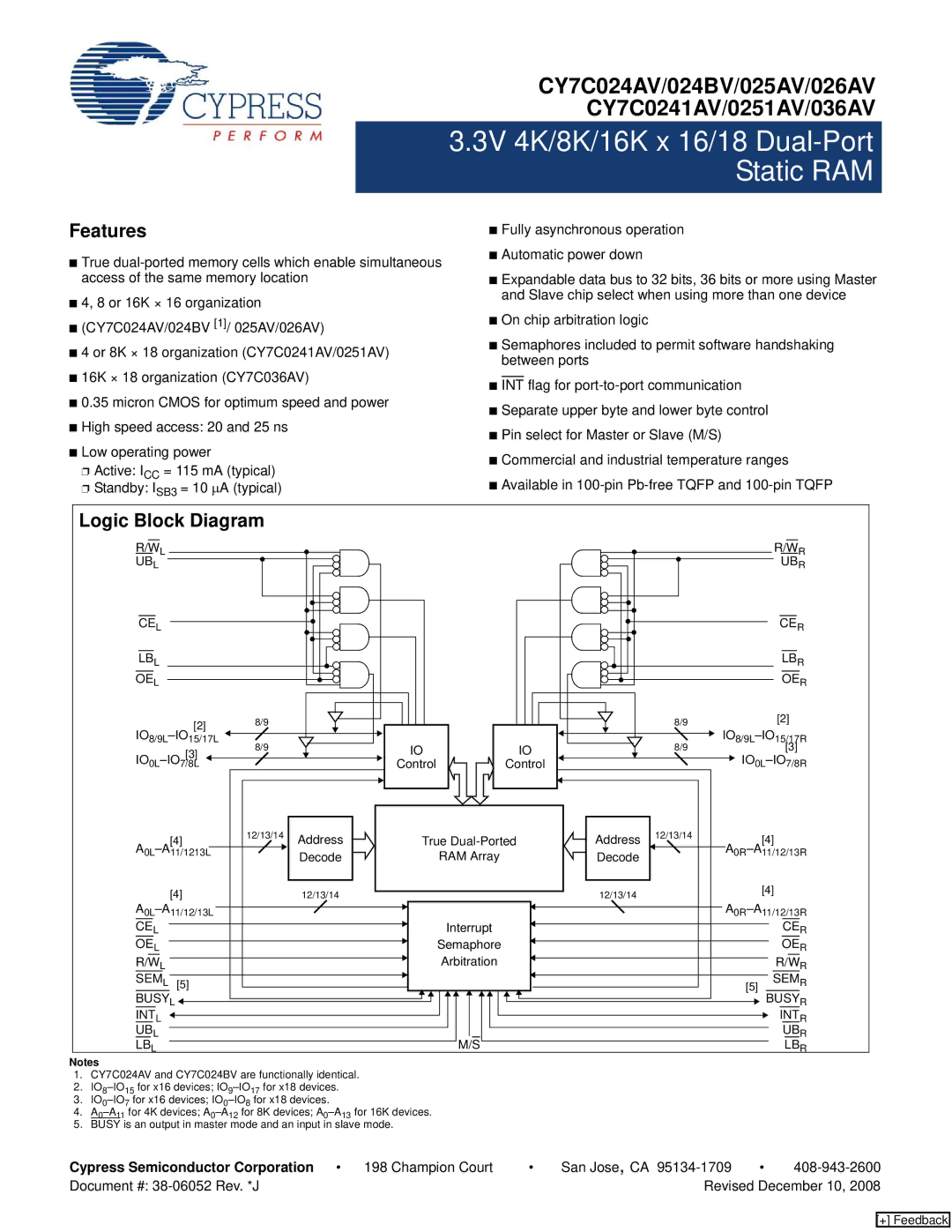
Logic Block Diagram
R/WL
UBL
CEL
LBL
OEL
IO |
| [2] |
| 8/9 |
|
| ||
|
|
|
| |||||
|
|
|
|
| ||||
| 15/17L |
|
|
| ||||
| 8/9L |
| 8/9 |
|
| |||
IO | 0L | [3] |
|
|
| |||
|
|
|
| |||||
|
|
|
| |||||
|
| 7/8L |
|
|
| |||
IO
Control
IO
Control
R/WR
UBR
CER
LBR
OER
8/9[2]
8/9[3]
|
|
|
|
|
|
|
|
|
|
|
| 12/13/14 |
|
|
|
|
|
|
|
|
|
|
|
|
|
|
|
|
|
|
|
|
|
|
|
|
|
| 12/13/14 |
|
|
|
|
|
|
|
|
|
|
|
|
|
|
| |||
| Address |
|
|
|
| True |
|
|
|
| Address |
|
|
|
| ||||||||||||||||||||||||||||||||||||||||||
|
|
|
|
|
|
|
|
|
|
|
|
|
|
|
|
|
| ||||||||||||||||||||||||||||||||||||||||
|
|
|
|
|
|
|
|
|
|
|
|
| |||||||||||||||||||||||||||||||||||||||||||||
|
|
|
| Decode |
|
|
|
|
|
|
| RAM Array |
|
|
|
| Decode |
| |||||||||||||||||||||||||||||||||||||||
[4] |
|
|
|
|
|
|
|
|
|
|
|
|
|
|
|
|
|
| [4] |
|
|
| |||||||||||||||||||||||||||||||||||
|
|
|
|
|
|
|
|
|
|
|
|
|
|
|
|
|
|
|
|
|
|
|
|
|
|
|
|
|
|
|
|
|
|
| |||||||||||||||||||||||
|
|
|
|
|
|
|
|
|
|
|
|
|
|
|
|
|
|
|
|
|
|
|
|
|
|
|
|
|
|
|
|
|
|
| |||||||||||||||||||||||
|
|
|
|
|
| 12/13/14 |
|
|
|
|
|
|
|
|
|
|
|
|
|
|
|
|
|
|
| 12/13/14 |
| ||||||||||||||||||||||||||||||
|
|
|
|
|
|
|
|
|
|
|
|
|
|
|
|
|
|
|
|
|
|
|
|
|
|
|
|
|
|
|
|
|
|
|
|
|
|
|
|
|
| ||||||||||||||||
|
|
|
|
|
|
|
|
|
|
|
|
|
|
|
|
|
|
|
|
|
|
|
|
|
|
|
|
|
|
|
|
| |||||||||||||||||||||||||
CE |
|
|
|
|
|
|
|
|
|
|
|
|
|
|
|
|
|
|
|
| Interrupt |
|
|
|
|
|
|
|
|
|
|
|
|
|
|
|
|
|
|
| CER | ||||||||||||||||
L |
|
|
|
|
|
|
|
|
|
|
|
|
|
|
|
|
|
|
|
|
|
|
|
|
|
|
|
|
|
|
| ||||||||||||||||||||||||||
OE |
|
|
|
|
|
|
|
|
|
|
|
|
|
|
|
|
|
|
| Semaphore |
|
|
|
|
|
|
|
|
|
|
|
|
|
|
|
|
|
|
| OE | R | ||||||||||||||||
L |
|
|
|
|
|
|
|
|
|
|
|
|
|
|
|
|
|
|
|
|
|
|
|
|
|
|
|
|
|
| |||||||||||||||||||||||||||
|
|
|
|
|
|
|
|
|
|
|
|
|
|
|
|
|
|
|
|
|
| Arbitration |
|
|
|
|
|
|
|
|
|
|
|
|
|
|
|
|
|
|
|
|
| ||||||||||||||
R/W |
|
|
|
|
|
|
|
|
|
|
|
|
|
|
|
|
|
|
|
|
|
|
|
| R/W | R | |||||||||||||||||||||||||||||||
L |
|
|
|
|
|
|
|
|
|
|
|
|
|
|
|
|
|
|
|
|
|
| |||||||||||||||||||||||||||||||||||
SEM | L |
|
|
|
|
|
|
|
|
|
|
|
|
|
|
|
|
|
|
|
|
|
|
|
|
|
|
|
|
|
|
|
|
|
|
|
|
|
|
|
|
|
|
|
|
| SEM | R | |||||||||
[5] |
|
|
|
|
|
|
|
|
|
|
|
|
|
|
|
|
|
|
|
|
|
|
|
|
|
|
|
|
|
|
|
| [5] |
|
| ||||||||||||||||||||||
|
|
|
|
|
|
|
|
|
|
|
|
|
|
|
|
|
|
|
|
|
|
|
|
|
|
|
|
|
|
|
|
|
|
|
|
| |||||||||||||||||||||
BUSY | L |
|
|
|
|
|
|
|
|
|
|
|
|
|
|
|
|
|
|
|
|
|
|
|
|
|
|
|
|
|
|
|
|
|
|
|
|
|
|
| BUSY | R | |||||||||||||||
INTL |
|
|
|
|
|
|
|
|
|
|
|
|
|
|
|
|
|
|
|
|
|
|
|
|
|
|
|
|
|
|
|
|
|
|
|
|
|
|
|
|
|
|
|
| INTR | ||||||||||||
|
|
|
|
|
|
|
|
|
|
|
|
|
|
|
|
|
|
|
|
|
|
|
|
|
|
|
|
|
|
|
|
|
|
|
|
|
| ||||||||||||||||||||
UBL |
|
|
|
|
|
|
|
|
|
|
|
|
|
|
|
|
|
|
|
|
|
|
|
|
|
|
|
|
|
|
|
|
|
|
|
|
|
|
|
|
|
|
|
|
| UBR | |||||||||||
|
|
|
|
|
|
|
|
|
|
|
|
|
|
|
|
|
|
|
|
|
|
|
|
|
|
|
|
|
|
|
|
|
|
|
|
|
|
|
|
| |||||||||||||||||
LBL |
|
|
|
|
|
|
|
|
|
|
|
|
|
|
|
|
| M/S |
|
|
|
|
|
|
|
|
|
|
|
|
|
|
|
|
|
|
|
|
|
|
|
|
| LBR | |||||||||||||
|
|
|
|
|
|
|
|
|
|
|
|
|
|
|
|
|
|
|
|
|
|
|
|
|
|
|
|
|
|
|
|
|
|
|
|
|
| ||||||||||||||||||||
Notes
1.CY7C024AV and CY7C024BV are functionally identical.
2.
3.
4.
5.BUSY is an output in master mode and an input in slave mode.
Cypress Semiconductor Corporation • 198 Champion Court | • | San Jose, CA | • | |
Document #: |
| Revised December 10, 2008 | ||
[+] Feedback