CY7C024AV/024BV/025AV/026AV
CY7C0241AV/0251AV/036AV
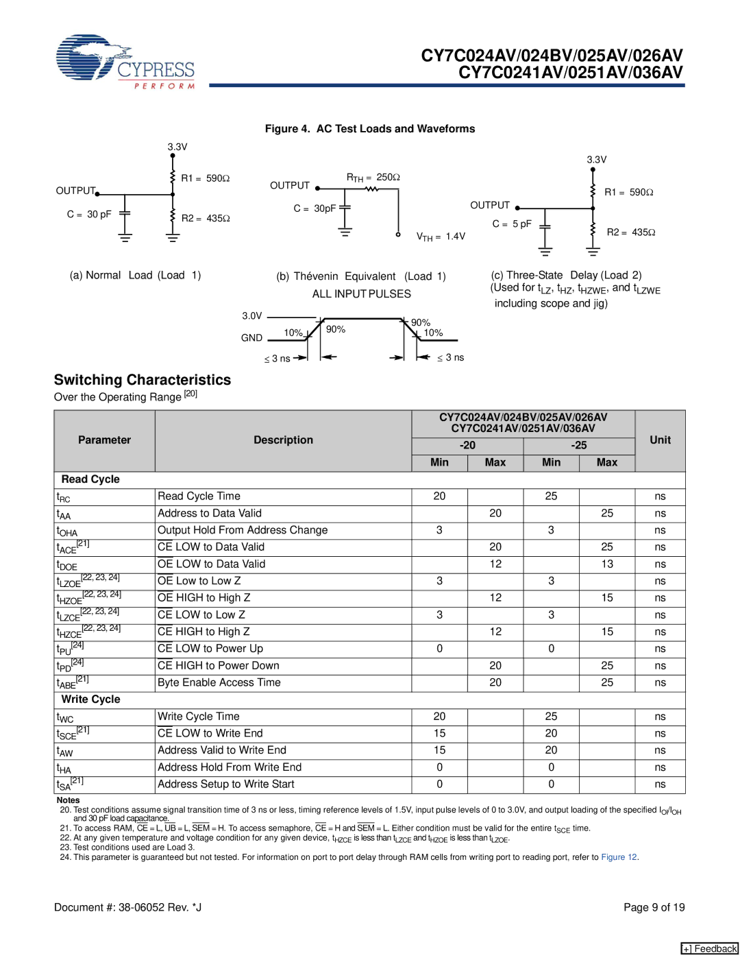
Figure 4. AC Test Loads and Waveforms
OUTPUT
C = 30 pF
3.3V
R1 = 590Ω | OUTPUT |
|
|
|
|
| RTH = 250Ω | ||||
R2 = 435Ω | C = 30pF |
|
|
|
|
|
|
| OUTPUT | ||
|
|
|
|
| |||||||
|
|
|
|
|
|
|
|
|
| C = 5 pF | |
|
|
|
|
|
|
|
|
|
|
| |
|
|
|
|
|
|
|
|
|
|
| VTH = 1.4V |
|
|
|
|
|
|
|
|
|
|
| |
|
|
|
|
|
|
|
|
|
|
| |
3.3V
R1 = 590Ω
R2 = 435Ω
(a) Normal Load (Load 1) |
|
| (b) Thévenin Equivalent | (Load 1) | ||||||||||||||
|
|
|
|
|
| ALL INPUTPULSES | ||||||||||||
| 3.0V |
|
|
|
|
|
|
|
|
|
|
|
| 90% | ||||
| GND | 10% |
|
|
|
|
|
| 90% |
|
|
|
|
| 10% | |||
|
|
|
|
|
|
|
|
|
|
| ||||||||
|
|
|
|
|
|
|
|
|
|
|
|
|
|
|
|
| ≤ 3 ns | |
|
| ≤ 3 ns |
|
|
|
|
|
|
|
|
|
|
|
|
| |||
|
|
|
|
|
|
|
|
|
|
| ||||||||
(c)
Switching Characteristics
Over the Operating Range [20]
|
|
|
|
|
| CY7C024AV/024BV/025AV/026AV |
| |||||
| Parameter |
|
|
| Description | CY7C0241AV/0251AV/036AV |
| Unit | ||||
|
|
|
|
|
| |||||||
|
|
|
|
|
|
|
|
| ||||
|
|
|
|
|
| Min |
| Max | Min |
| Max |
|
| Read Cycle |
|
|
|
|
|
|
|
|
|
|
|
tRC |
| Read Cycle Time | 20 |
|
| 25 |
|
| ns | |||
tAA |
| Address to Data Valid |
|
| 20 |
|
| 25 | ns | |||
tOHA |
| Output Hold From Address Change | 3 |
|
| 3 |
|
| ns | |||
tACE[21] |
| CE |
| LOW to Data Valid |
|
| 20 |
|
| 25 | ns | |
tDOE |
| OE | LOW to Data Valid |
|
| 12 |
|
| 13 | ns | ||
tLZOE[22, 23, 24] |
| OE | Low to Low Z | 3 |
|
| 3 |
|
| ns | ||
tHZOE[22, 23, 24] |
| OE | HIGH to High Z |
|
| 12 |
|
| 15 | ns | ||
tLZCE[22, 23, 24] |
| CE | LOW to Low Z | 3 |
|
| 3 |
|
| ns | ||
tHZCE[22, 23, 24] |
| CE | HIGH to High Z |
|
| 12 |
|
| 15 | ns | ||
t | [24] |
| CE | LOW to Power Up | 0 |
|
| 0 |
|
| ns | |
| PU |
|
|
|
|
|
|
|
|
|
|
|
t | [24] |
| CE | HIGH to Power Down |
|
| 20 |
|
| 25 | ns | |
| PD |
|
|
|
|
|
|
|
|
|
|
|
tABE[21] |
| Byte Enable Access Time |
|
| 20 |
|
| 25 | ns | |||
| Write Cycle |
|
|
|
|
|
|
|
|
|
|
|
tWC |
| Write Cycle Time | 20 |
|
| 25 |
|
| ns | |||
tSCE[21] |
| CE | LOW to Write End | 15 |
|
| 20 |
|
| ns | ||
tAW |
| Address Valid to Write End | 15 |
|
| 20 |
|
| ns | |||
tHA |
| Address Hold From Write End | 0 |
|
| 0 |
|
| ns | |||
t | [21] |
| Address Setup to Write Start | 0 |
|
| 0 |
|
| ns | ||
| SA |
|
|
|
|
|
|
|
|
|
|
|
Notes |
|
|
|
|
|
|
|
|
|
| ||
20.Test conditions assume signal transition time of 3 ns or less, timing reference levels of 1.5V, input pulse levels of 0 to 3.0V, and output loading of the specified IOI/IOH and 30 pF load capacitance.
21.To access RAM, CE = L, UB = L, SEM = H. To access semaphore, CE = H and SEM = L. Either condition must be valid for the entire tSCE time.
22.At any given temperature and voltage condition for any given device, tHZCE is less than tLZCE and tHZOE is less than tLZOE.
23.Test conditions used are Load 3.
24.This parameter is guaranteed but not tested. For information on port to port delay through RAM cells from writing port to reading port, refer to Figure 12.
Document #: | Page 9 of 19 |
[+] Feedback