CY7C1241V18, CY7C1256V18
CY7C1243V18, CY7C1245V18
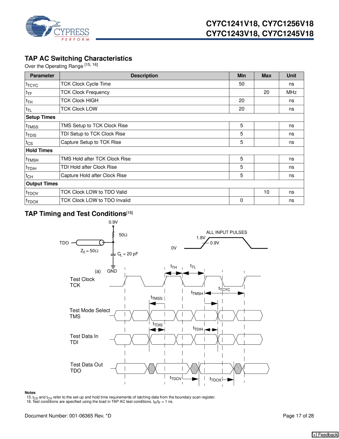
TAP AC Switching Characteristics
Over the Operating Range [15, 16]
Parameter | Description | Min | Max | Unit |
tTCYC | TCK Clock Cycle Time | 50 |
| ns |
tTF | TCK Clock Frequency |
| 20 | MHz |
tTH | TCK Clock HIGH | 20 |
| ns |
tTL | TCK Clock LOW | 20 |
| ns |
Setup Times |
|
|
|
|
|
|
|
|
|
tTMSS | TMS Setup to TCK Clock Rise | 5 |
| ns |
tTDIS | TDI Setup to TCK Clock Rise | 5 |
| ns |
tCS | Capture Setup to TCK Rise | 5 |
| ns |
Hold Times |
|
|
|
|
|
|
|
|
|
tTMSH | TMS Hold after TCK Clock Rise | 5 |
| ns |
tTDIH | TDI Hold after Clock Rise | 5 |
| ns |
tCH | Capture Hold after Clock Rise | 5 |
| ns |
Output Times |
|
|
|
|
|
|
|
|
|
tTDOV | TCK Clock LOW to TDO Valid |
| 10 | ns |
tTDOX | TCK Clock LOW to TDO Invalid | 0 |
| ns |
0V
tTH
ALL INPUT PULSES
1.8V
0.9V
tTL
tTCYC
tTMSH ![]()
Test Mode Select
TMS
Test Data In
TDI
Test Data Out
TDO
tTDIS | tTDIH |
|
tTDOV |
|
|
|
| t |
|
|
|
| ||
|
|
|
| ||
|
|
|
| ||
|
|
|
| ||
|
|
|
| ||
|
|
|
| ||
|
|
|
| ||
| |||||
|
|
|
| ||
|
|
|
|
| TDOX |
|
|
|
|
|
|
|
|
|
|
|
|
Notes
15.tCS and tCH refer to the
16.Test conditions are specified using the load in TAP AC test conditions. tR/tF = 1 ns.
Document Number: | Page 17 of 28 |
[+] Feedback