CY7C1241V18, CY7C1256V18
CY7C1243V18, CY7C1245V18
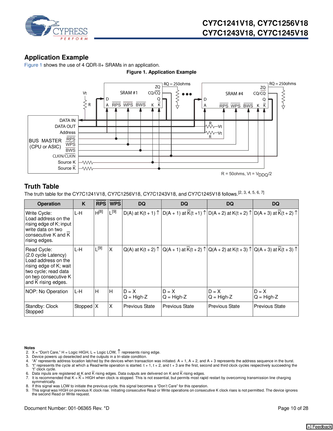
Application Example
Figure 1 shows the use of 4 QDR-II+ SRAMs in an application.
Figure 1. Application Example
|
|
| SRAM #1 |
| ZQ | RQ = 250ohms |
|
| ZQ | RQ = 250ohms |
| Vt |
| CQ/CQ |
|
| SRAM #4 | CQ/CQ |
| ||
|
| D | RPS WPS BWS |
| Q |
| D |
| Q |
|
| R | A | K | K |
| A | RPS WPS BWS | K K |
| |
DATA IN |
|
|
|
|
|
| R |
|
| |
DATA OUT |
|
|
|
|
|
|
|
| ||
|
|
|
|
|
| Vt |
|
| ||
Address |
|
|
|
|
|
| Vt |
|
| |
BUS MASTER | RPS |
|
|
|
|
|
| R |
|
|
|
|
|
|
|
|
|
|
| ||
(CPU or ASIC) | WPS |
|
|
|
|
|
|
|
|
|
| BWS |
|
|
|
|
|
|
|
|
|
CLKIN/CLKIN |
|
|
|
|
|
|
|
|
| |
Source K |
|
|
|
|
|
|
|
|
| |
Source K |
|
|
|
|
|
| R = 50ohms, Vt = VDDQ/2 | |||
|
|
|
|
|
|
|
| |||
Truth Table
The truth table for the CY7C1241V18, CY7C1256V18, CY7C1243V18, and CY7C1245V18 follows.[2, 3, 4, 5, 6, 7]
Operation | K | RPS | WPS | DQ | DQ | DQ | DQ | |||||||||
Write Cycle: | H[8] | L[9] | D(A) at K(t + 1) ↑ | D(A + 1) at |
|
|
| D(A + 2) at K(t + 2) ↑ |
|
|
|
| ||||
K(t +1) ↑ | D(A + 3) at K(t + 2) ↑ | |||||||||||||||
Load address on the |
|
|
|
|
|
|
|
|
|
|
|
|
|
| ||
rising edge of K; input |
|
|
|
|
|
|
|
|
|
|
|
|
|
| ||
write data on two |
|
|
|
|
|
|
|
|
|
|
|
|
|
| ||
consecutive K and | K |
|
|
|
|
|
|
|
|
|
|
|
|
|
|
|
rising edges. |
|
|
|
|
|
|
|
|
|
|
|
|
|
| ||
|
|
|
|
|
|
|
|
|
|
| ||||||
Read Cycle: | L[9] | X | Q(A) at K(t + 2) ↑ | Q(A + 1) at |
|
|
|
| Q(A + 2) at K(t + 3) ↑ |
|
|
|
| |||
K(t + 2) ↑ | Q(A + 3) at K(t + 3) ↑ | |||||||||||||||
(2.0 cycle Latency) |
|
|
|
|
|
|
|
|
|
|
|
|
|
| ||
Load address on the |
|
|
|
|
|
|
|
|
|
|
|
|
|
| ||
rising edge of K; wait |
|
|
|
|
|
|
|
|
|
|
|
|
|
| ||
two cycle; read data |
|
|
|
|
|
|
|
|
|
|
|
|
|
| ||
on two consecutive K |
|
|
|
|
|
|
|
|
|
|
|
|
|
| ||
and K rising edges. |
|
|
|
|
|
|
|
|
|
|
|
|
|
| ||
|
|
|
|
|
|
|
| |||||||||
NOP: No Operation | H | H | D = X | D = X | D = X | D = X | ||||||||||
|
|
|
|
|
| Q = | Q = | Q = | Q = | |||||||
|
|
|
|
|
|
|
| |||||||||
Standby: Clock | Stopped | X | X | Previous State | Previous State | Previous State | Previous State | |||||||||
Stopped |
|
|
|
|
|
|
|
|
|
|
|
|
|
| ||
|
|
|
|
|
|
|
|
|
|
|
|
|
|
|
|
|
Notes
2.X = “Don't Care,” H = Logic HIGH, L = Logic LOW, ↑ represents rising edge.
3.Device powers up deselected and the outputs in a
4.“A” represents address location latched by the devices when transaction was initiated. A + 1, A + 2, and A + 3 represents the address sequence in the burst.
5.“t” represents the cycle at which a Read/write operation is started. t + 1, t + 2, and t + 3 are the first, second and third clock cycles respectively succeeding the “t” clock cycle.
6.Data inputs are registered at K and K rising edges. Data outputs are delivered on K and K rising edges.
7.It is recommended that K = K = HIGH when clock is stopped. This is not essential, but permits most rapid restart by overcoming transmission line charging symmetrically.
8.If this signal was LOW to initiate the previous cycle, this signal becomes a “Don’t Care” for this operation.
9.This signal was HIGH on previous K clock rise. Initiating consecutive Read or Write operations on consecutive K clock rises is not permitted. The device ignores the second Read or Write request.
Document Number: | Page 10 of 28 |
[+] Feedback