|
|
|
|
|
|
|
|
|
|
|
|
|
|
|
|
| CY7C1241V18, CY7C1256V18 | |||||||||||
|
|
|
|
|
|
|
|
|
|
|
|
|
|
|
|
| CY7C1243V18, CY7C1245V18 | |||||||||||
|
|
|
|
|
|
|
|
|
|
|
|
|
|
|
|
|
|
|
|
|
|
|
|
|
|
|
| |
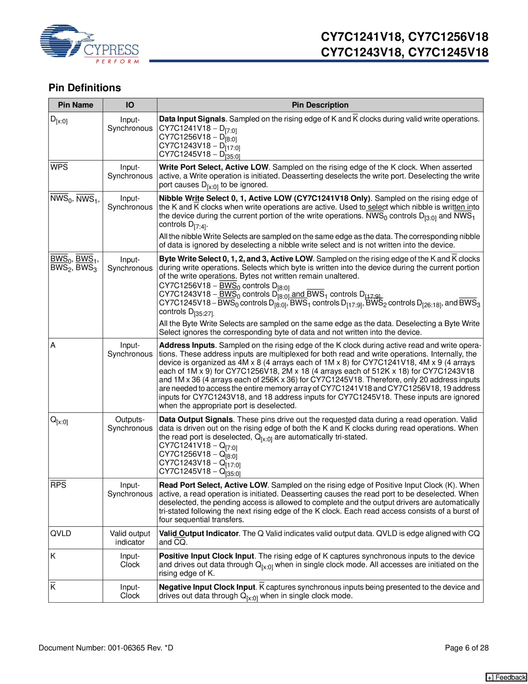
| Pin Definitions |
|
|
|
|
|
|
|
|
|
|
|
|
|
|
|
| |||||||||||
|
|
|
|
|
|
|
|
|
|
|
|
|
|
|
|
|
|
|
|
|
|
|
|
|
| |||
|
| Pin Name | IO |
|
|
| Pin Description |
|
| |||||||||||||||||||
| D[x:0] | Input- | Data Input Signals. Sampled on the rising edge of K and |
| clocks during valid write operations. |
| ||||||||||||||||||||||
| K | |||||||||||||||||||||||||||
|
|
|
|
|
|
|
|
|
| Synchronous | CY7C1241V18 − D[7:0] |
|
|
|
|
|
|
|
|
|
|
|
|
|
|
| ||
|
|
|
|
|
|
|
|
|
|
|
|
| CY7C1256V18 − D[8:0] |
|
|
|
|
|
|
|
|
|
|
|
|
|
|
|
|
|
|
|
|
|
|
|
|
|
|
|
| CY7C1243V18 − D[17:0] |
|
|
|
|
|
|
|
|
|
|
|
|
|
|
|
|
|
|
|
|
|
|
|
|
|
|
|
| CY7C1245V18 − D[35:0] |
|
|
|
|
|
|
|
|
|
|
|
|
|
|
|
|
|
|
|
|
|
|
|
|
| Input- | Write Port Select, Active LOW. Sampled on the rising edge of the K clock. When asserted |
| ||||||||||||||||
| WPS | |||||||||||||||||||||||||||
|
|
|
|
|
|
|
|
|
| Synchronous | active, a Write operation is initiated. Deasserting deselects the write port. Deselecting the write |
| ||||||||||||||||
|
|
|
|
|
|
|
|
|
|
|
|
| port causes D[x:0] to be ignored. |
| ||||||||||||||
|
|
|
|
| 0, |
|
|
| 1, | Input- | Nibble Write Select 0, 1, Active LOW (CY7C1241V18 Only). Sampled on the rising edge of |
| ||||||||||||||||
| NWS | |||||||||||||||||||||||||||
| NWS | |||||||||||||||||||||||||||
|
|
|
|
|
|
|
|
|
| Synchronous | the K and K clocks when write operations are active. Used to select which nibble is written into |
| ||||||||||||||||
|
|
|
|
|
|
|
|
|
|
|
|
| the device during the current portion of the write operations. NWS0 controls D[3:0] and NWS1 |
| ||||||||||||||
|
|
|
|
|
|
|
|
|
|
|
|
| controls D[7:4]. |
|
|
|
|
|
|
|
|
|
|
|
|
|
|
|
|
|
|
|
|
|
|
|
|
|
|
|
| All the nibble Write Selects are sampled on the same edge as the data. The corresponding nibble |
| ||||||||||||||
|
|
|
|
|
|
|
|
|
|
|
|
| of data is ignored by deselecting a nibble write select and is not written into the device. |
| ||||||||||||||
|
|
|
| 0, |
|
| 1, | Input- | Byte Write Select 0, 1, 2, and 3, Active LOW. Sampled on the rising edge of the K and |
| clocks |
| ||||||||||||||||
| BWS | BWS | K | |||||||||||||||||||||||||
| BWS2, BWS3 | Synchronous | during write operations. Selects which byte is written into the device during the current portion |
| ||||||||||||||||||||||||
|
|
|
|
|
|
|
|
|
|
|
|
| of the write operations. Bytes not written remain unaltered. |
| ||||||||||||||
|
|
|
|
|
|
|
|
|
|
|
|
| CY7C1256V18 − BWS0 | controls D[8:0] |
| |||||||||||||
|
|
|
|
|
|
|
|
|
|
|
|
| CY7C1243V18 − BWS0 | controls D[8:0] and | BWS | 1 controls D | [17:9]. |
|
|
|
| |||||||
|
|
|
|
|
|
|
|
|
|
|
|
| CY7C1245V18 − BWS0 controls D[8:0], BWS1 controls D[17:9], BWS2 controls D[26:18], and BWS3 |
| ||||||||||||||
|
|
|
|
|
|
|
|
|
|
|
|
| controls D[35:27]. |
|
|
|
|
|
|
|
|
|
|
|
|
|
|
|
|
|
|
|
|
|
|
|
|
|
|
|
| All the Byte Write Selects are sampled on the same edge as the data. Deselecting a Byte Write |
| ||||||||||||||
|
|
|
|
|
|
|
|
|
|
|
|
| Select ignores the corresponding byte of data and not written into the device. |
| ||||||||||||||
| A | Input- | Address Inputs. Sampled on the rising edge of the K clock during active read and write opera- |
|
| |||||||||||||||||||||||
|
|
|
|
|
|
|
|
|
| Synchronous | tions. These address inputs are multiplexed for both read and write operations. Internally, the |
| ||||||||||||||||
|
|
|
|
|
|
|
|
|
|
|
|
| device is organized as 4M x 8 (4 arrays each of 1M x 8) for CY7C1241V18, 4M x 9 (4 arrays |
| ||||||||||||||
|
|
|
|
|
|
|
|
|
|
|
|
| each of 1M x 9) for CY7C1256V18, 2M x 18 (4 arrays each of 512K x 18) for CY7C1243V18 |
| ||||||||||||||
|
|
|
|
|
|
|
|
|
|
|
|
| and 1M x 36 (4 arrays each of 256K x 36) for CY7C1245V18. Therefore, only 20 address inputs |
| ||||||||||||||
|
|
|
|
|
|
|
|
|
|
|
|
| are needed to access the entire memory array of CY7C1241V18 and CY7C1256V18, 19 address |
| ||||||||||||||
|
|
|
|
|
|
|
|
|
|
|
|
| inputs for CY7C1243V18, and 18 address inputs for CY7C1245V18. These inputs are ignored |
| ||||||||||||||
|
|
|
|
|
|
|
|
|
|
|
|
| when the appropriate port is deselected. |
| ||||||||||||||
| Q[x:0] | Outputs- | Data Output Signals. These pins drive out the requested data during a read operation. Valid |
|
| |||||||||||||||||||||||
|
|
|
|
|
|
|
|
|
| Synchronous | data is driven out on the rising edge of both the K and K clocks during read operations. When |
| ||||||||||||||||
|
|
|
|
|
|
|
|
|
|
|
|
| the read port is deselected, Q[x:0] are automatically |
| ||||||||||||||
|
|
|
|
|
|
|
|
|
|
|
|
| CY7C1241V18 − Q[7:0] |
|
|
|
|
|
|
|
|
|
|
|
|
|
|
|
|
|
|
|
|
|
|
|
|
|
|
|
| CY7C1256V18 − Q[8:0] |
|
|
|
|
|
|
|
|
|
|
|
|
|
|
|
|
|
|
|
|
|
|
|
|
|
|
|
| CY7C1243V18 − Q[17:0] |
|
|
|
|
|
|
|
|
|
|
|
|
|
|
|
|
|
|
|
|
|
|
|
|
|
|
|
| CY7C1245V18 − Q[35:0] |
|
|
|
|
|
|
|
|
|
|
|
|
|
|
|
|
|
|
| Input- | Read Port Select, Active LOW. Sampled on the rising edge of Positive Input Clock (K). When |
| ||||||||||||||||||||||
| RPS | |||||||||||||||||||||||||||
|
|
|
|
|
|
|
|
|
| Synchronous | active, a read operation is initiated. Deasserting causes the read port to be deselected. When |
| ||||||||||||||||
|
|
|
|
|
|
|
|
|
|
|
|
| deselected, the pending access is allowed to complete and the output drivers are automatically |
| ||||||||||||||
|
|
|
|
|
|
|
|
|
|
|
|
|
| |||||||||||||||
|
|
|
|
|
|
|
|
|
|
|
|
| four sequential transfers. |
| ||||||||||||||
| QVLD | Valid output | Valid Output Indicator. The Q Valid indicates valid output data. QVLD is edge aligned with CQ |
|
| |||||||||||||||||||||||
|
|
|
|
|
|
|
|
|
| indicator | and CQ. |
|
|
|
|
|
|
|
|
|
|
|
|
|
|
| ||
| K | Input- | Positive Input Clock Input. The rising edge of K captures synchronous inputs to the device |
|
| |||||||||||||||||||||||
|
|
|
|
|
|
|
|
|
| Clock | and drives out data through Q[x:0] when in single clock mode. All accesses are initiated on the |
| ||||||||||||||||
|
|
|
|
|
|
|
|
|
|
|
|
| rising edge of K. |
|
|
|
|
|
|
|
|
|
|
|
|
|
|
|
|
|
| Input- | Negative Input Clock Input. |
| captures synchronous inputs being presented to the device and |
| |||||||||||||||||||||
| K | K | ||||||||||||||||||||||||||
|
|
|
|
|
|
|
|
|
| Clock | drives out data through Q[x:0] when in single clock mode. |
| ||||||||||||||||
Document Number: | Page 6 of 28 |
[+] Feedback