CY7C1241V18, CY7C1256V18 CY7C1243V18, CY7C1245V18
Maximum Ratings
Exceeding maximum ratings may shorten the useful life of the device. User guidelines are not tested.
Storage Temperature .................................
Ambient Temperature with Power Applied..
Supply Voltage on VDD Relative to GND | ||
Supply Voltage on VDDQ Relative to GND | ||
DC Applied to Outputs in | ||
DC Input Voltage[13] | ||
|
| DD |
Current into Outputs (LOW) |
|
|
| 20 mA | |
Static Discharge Voltage | >2001V | ||||
Latch Up Current |
|
|
| >200 mA | |
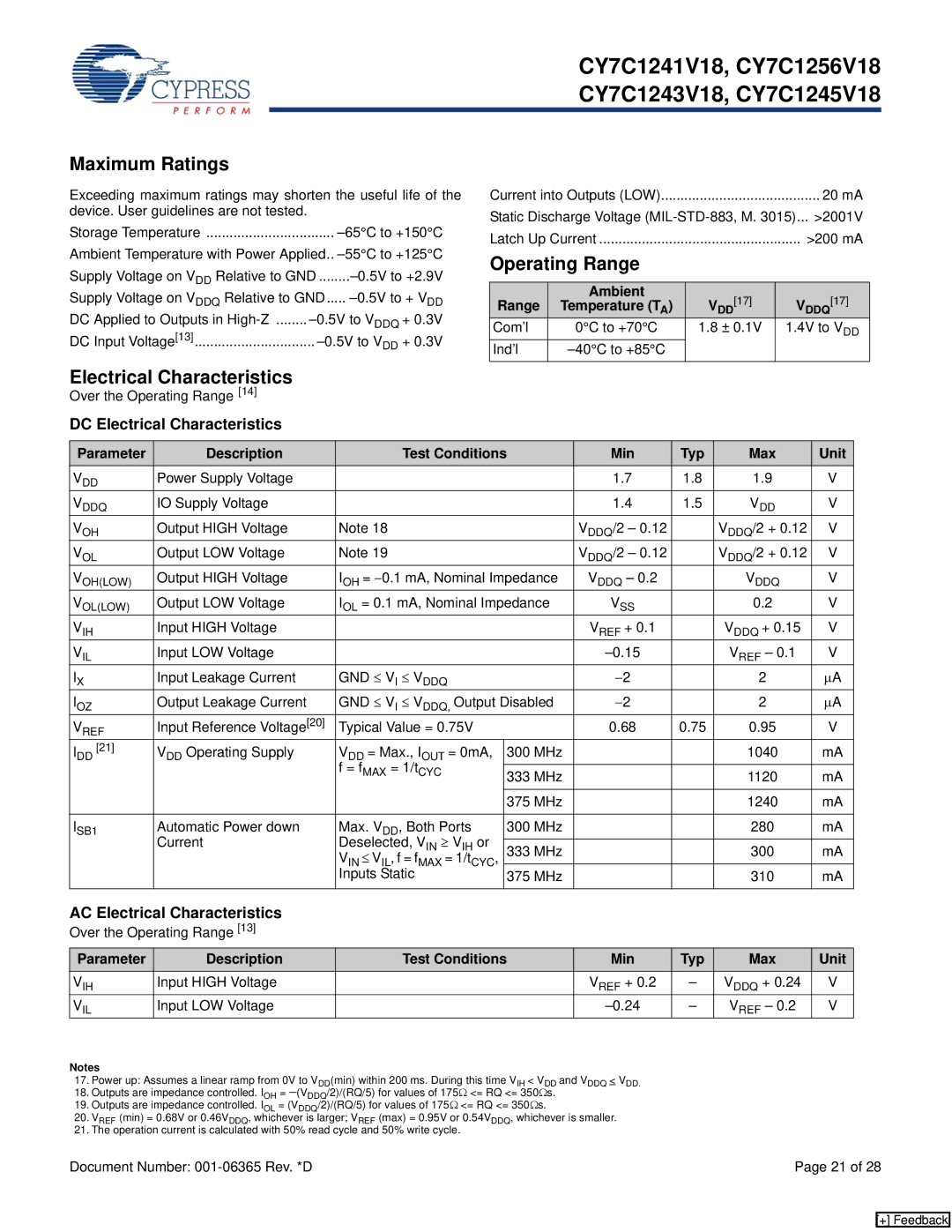
Operating Range |
|
|
|
| |
|
|
|
|
|
|
Range | Ambient | V | [17] | V | [17] |
Temperature (T ) | |||||
| A |
| DD |
| DDQ |
Com’l | 0°C to +70°C | 1.8 | ± 0.1V | 1.4V to VDD | |
Ind’l |
|
|
|
| |
|
|
|
|
|
|
Electrical Characteristics
Over the Operating Range [14]
DC Electrical Characteristics
Parameter | Description |
|
| Test Conditions | Min | Typ | Max | Unit | ||||
VDD | Power Supply Voltage |
|
|
|
|
|
|
| 1.7 | 1.8 | 1.9 | V |
VDDQ | IO Supply Voltage |
|
|
|
|
|
|
| 1.4 | 1.5 | VDD | V |
VOH | Output HIGH Voltage | Note 18 |
|
|
|
| VDDQ/2 – 0.12 |
| VDDQ/2 + 0.12 | V | ||
VOL | Output LOW Voltage | Note 19 |
|
|
|
| VDDQ/2 – 0.12 |
| VDDQ/2 + 0.12 | V | ||
VOH(LOW) | Output HIGH Voltage | IOH = −0.1 mA, Nominal Impedance | VDDQ – 0.2 |
| VDDQ | V | ||||||
VOL(LOW) | Output LOW Voltage | IOL = 0.1 mA, Nominal Impedance | VSS |
| 0.2 | V | ||||||
VIH | Input HIGH Voltage |
|
|
|
|
|
|
| VREF + 0.1 |
| VDDQ + 0.15 | V |
VIL | Input LOW Voltage |
|
|
|
|
|
|
|
| VREF – 0.1 | V | |
IX | Input Leakage Current | GND ≤ VI ≤ VDDQ |
|
|
| −2 |
| 2 | μA | |||
IOZ | Output Leakage Current | GND ≤ VI ≤ VDDQ, Output Disabled | −2 |
| 2 | μA | ||||||
VREF | Input Reference Voltage[20] | Typical Value = 0.75V |
|
| 0.68 | 0.75 | 0.95 | V | ||||
IDD [21] | VDD Operating Supply | VDD = Max., IOUT = 0mA, |
| 300 MHz |
|
| 1040 | mA | ||||
|
| f = fMAX = 1/tCYC |
|
|
|
|
|
|
| |||
|
|
|
| 333 MHz |
|
| 1120 | mA | ||||
|
|
|
|
|
|
|
| 375 MHz |
|
| 1240 | mA |
|
|
|
|
|
|
|
|
| ||||
ISB1 | Automatic Power down | Max. VDD, Both Ports |
| 300 MHz |
|
| 280 | mA | ||||
| Current | Deselected, VIN ≥ VIH or |
|
|
|
|
|
| ||||
|
| 333 MHz |
|
| 300 | mA | ||||||
|
| V |
| ≤ V , f = f | = 1/t |
| , |
|
| |||
|
|
| IN | IL | MAX | CYC |
|
|
|
|
|
|
|
| Inputs Static |
|
|
| 375 MHz |
|
| 310 | mA | ||
|
|
|
|
|
|
|
|
|
|
|
|
|
AC Electrical Characteristics
Over the Operating Range [13]
Parameter | Description | Test Conditions | Min | Typ | Max | Unit |
VIH | Input HIGH Voltage |
| VREF + 0.2 | – | VDDQ + 0.24 | V |
VIL | Input LOW Voltage |
| – | VREF – 0.2 | V |
Notes
17.Power up: Assumes a linear ramp from 0V to VDD(min) within 200 ms. During this time VIH < VDD and VDDQ < VDD.
18.Outputs are impedance controlled. IOH = −(VDDQ/2)/(RQ/5) for values of 175Ω <= RQ <= 350Ωs.
19.Outputs are impedance controlled. IOL = (VDDQ/2)/(RQ/5) for values of 175Ω <= RQ <= 350Ωs.
20.VREF (min) = 0.68V or 0.46VDDQ, whichever is larger; VREF (max) = 0.95V or 0.54VDDQ, whichever is smaller.
21.The operation current is calculated with 50% read cycle and 50% write cycle.
Document Number: | Page 21 of 28 |
[+] Feedback