HYUNDAI MicroElectronics | GMS90X5XC Series |
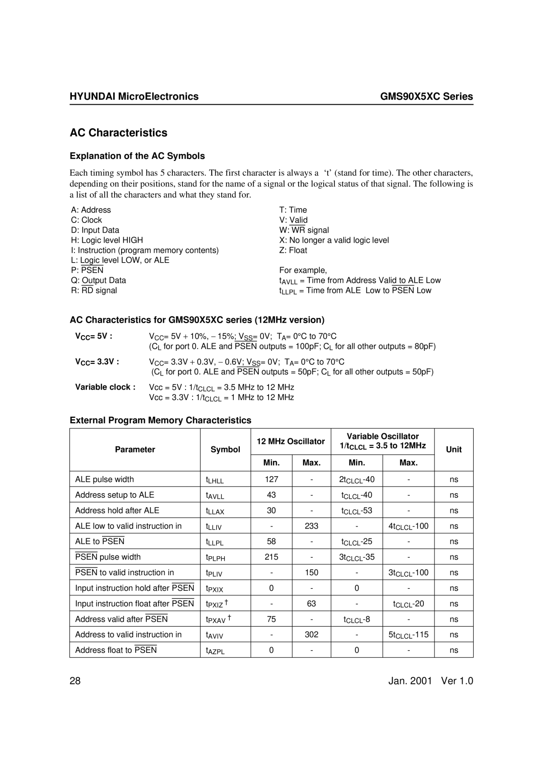
AC Characteristics
Explanation of the AC Symbols
Each timing symbol has 5 characters. The first character is always a ‘t’ (stand for time). The other characters, depending on their positions, stand for the name of a signal or the logical status of that signal. The following is a list of all the characters and what they stand for.
A:Address
C:Clock
D:Input Data
H:Logic level HIGH
I:Instruction (program memory contents)
L:Logic level LOW, or ALE
P:PSEN
Q:Output Data
R:RD signal
T:Time
V:Valid
W:WR signal
X:No longer a valid logic level
Z:Float
For example,
tAVLL = Time from Address Valid to ALE Low tLLPL = Time from ALE Low to PSEN Low
AC Characteristics for GMS90X5XC series (12MHz version)
VCC= 5V :VCC= 5V + 10%, − 15%; VSS= 0V; TA= 0°C to 70°C
(CL for port 0. ALE and PSEN outputs = 100pF; CL for all other outputs = 80pF)
VCC= 3.3V : VCC= 3.3V + 0.3V, − 0.6V; VSS= 0V; TA= 0°C to 70°C
(CL for port 0. ALE and PSEN outputs = 50pF; CL for all other outputs = 50pF)
Variable clock : Vcc = 5V : 1/tCLCL = 3.5 MHz to 12 MHz
Vcc = 3.3V : 1/tCLCL = 1 MHz to 12 MHz
External Program Memory Characteristics
|
|
|
|
|
|
|
|
|
|
|
|
| 12 MHz Oscillator | Variable Oscillator |
| ||
|
|
| Parameter | Symbol | 1/tCLCL = 3.5 to 12MHz | Unit | |||||||||||
|
|
|
|
| |||||||||||||
|
|
|
|
|
|
|
|
|
|
|
|
| Min. | Max. | Min. | Max. |
|
|
|
|
|
|
|
|
| ||||||||||
| ALE pulse width | tLHLL | 127 | - | - | ns | |||||||||||
| Address setup to ALE | tAVLL | 43 | - | - | ns | |||||||||||
| Address hold after ALE | tLLAX | 30 | - | - | ns | |||||||||||
|
|
|
|
|
|
|
| ||||||||||
| ALE low to valid instruction in | tLLIV | - | 233 | - | ns | |||||||||||
| ALE to |
|
|
|
|
|
|
|
|
| tLLPL | 58 | - | - | ns | ||
| PSEN |
|
|
|
|
|
|
|
| ||||||||
|
| pulse width | tPLPH | 215 | - | - | ns | ||||||||||
| PSEN | ||||||||||||||||
|
| to valid instruction in | tPLIV | - | 150 | - | ns | ||||||||||
| PSEN | ||||||||||||||||
| Input instruction hold after |
|
| tPXIX | 0 | - | 0 | - | ns | ||||||||
| PSEN |
| |||||||||||||||
| Input instruction float after |
|
|
| tPXIZ † | - | 63 | - | ns | ||||||||
| PSEN |
| |||||||||||||||
| Address valid after |
|
|
|
|
|
| tPXAV † | 75 | - | - | ns | |||||
| PSEN |
| |||||||||||||||
| Address to valid instruction in | tAVIV | - | 302 | - | ns | |||||||||||
| Address float to |
|
|
|
|
|
|
| tAZPL | 0 | - | 0 | - | ns | |||
| PSEN |
| |||||||||||||||
|
|
|
|
|
|
|
|
|
|
|
|
|
|
|
|
|
|
28 | Jan. 2001 Ver 1.0 |