GMS90X5XC Series |
|
|
| HYUNDAI MicroElectronics | |||||||
|
|
|
|
|
|
|
|
|
|
|
|
|
|
|
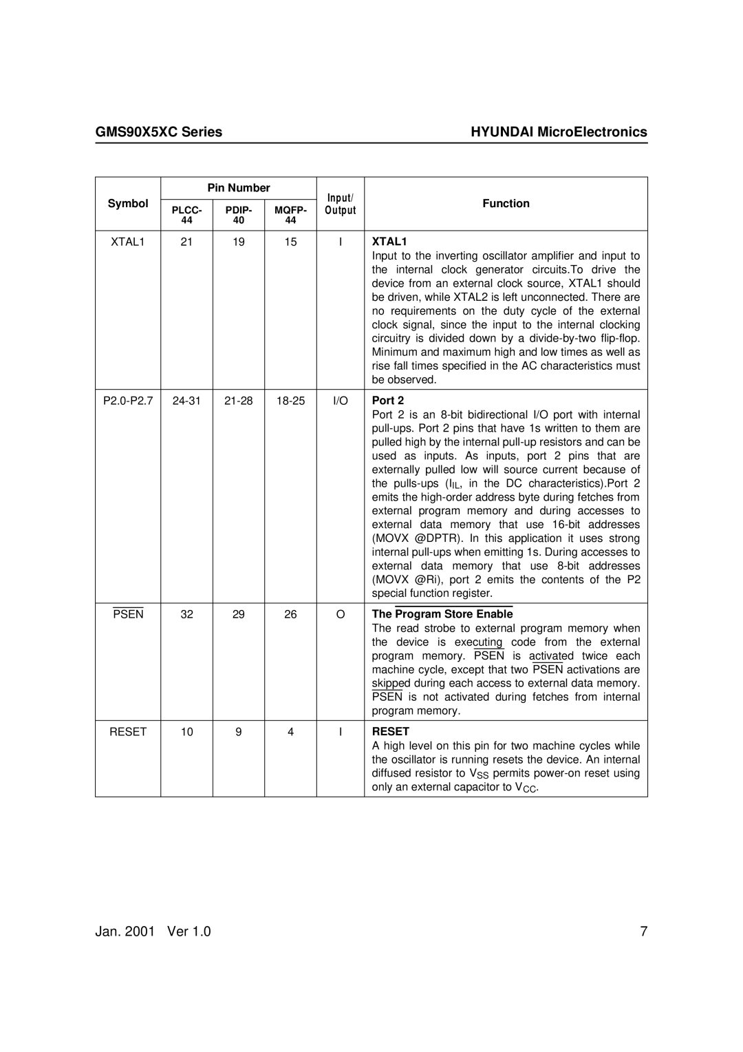
| Pin Number |
| Input/ |
|
|
| ||
Symbol |
|
|
|
|
|
| Function | ||||
PLCC- |
| PDIP- |
| MQFP- | Output |
| |||||
|
|
|
|
|
|
|
| ||||
|
|
| 44 |
| 40 |
| 44 |
|
|
|
|
|
|
|
|
|
|
|
| ||||
XTAL1 | 21 |
| 19 |
| 15 | I | XTAL1 | ||||
|
|
|
|
|
|
|
|
| Input to the inverting oscillator amplifier and input to | ||
|
|
|
|
|
|
|
|
| the internal clock generator circuits.To drive the | ||
|
|
|
|
|
|
|
|
| device from an external clock source, XTAL1 should | ||
|
|
|
|
|
|
|
|
| be driven, while XTAL2 is left unconnected. There are | ||
|
|
|
|
|
|
|
|
| no requirements on the duty cycle of the external | ||
|
|
|
|
|
|
|
|
| clock signal, since the input to the internal clocking | ||
|
|
|
|
|
|
|
|
| circuitry is divided down by a | ||
|
|
|
|
|
|
|
|
| Minimum and maximum high and low times as well as | ||
|
|
|
|
|
|
|
|
| rise fall times specified in the AC characteristics must | ||
|
|
|
|
|
|
|
|
| be observed. | ||
|
|
|
|
|
|
|
| ||||
|
| I/O | Port 2 | ||||||||
|
|
|
|
|
|
|
|
| Port 2 is an | ||
|
|
|
|
|
|
|
|
| |||
|
|
|
|
|
|
|
|
| pulled high by the internal | ||
|
|
|
|
|
|
|
|
| used as inputs. As inputs, port 2 pins that are | ||
|
|
|
|
|
|
|
|
| externally pulled low will source current because of | ||
|
|
|
|
|
|
|
|
| the | ||
|
|
|
|
|
|
|
|
| emits the | ||
|
|
|
|
|
|
|
|
| external program memory and during accesses to | ||
|
|
|
|
|
|
|
|
| external data memory that use | ||
|
|
|
|
|
|
|
|
| (MOVX @DPTR). In this application it uses strong | ||
|
|
|
|
|
|
|
|
| internal | ||
|
|
|
|
|
|
|
|
| external data memory that use | ||
|
|
|
|
|
|
|
|
| (MOVX @Ri), port 2 emits the contents of the P2 | ||
|
|
|
|
|
|
|
|
| special function register. | ||
|
|
|
|
|
|
|
|
| |||
|
|
|
|
|
|
|
|
|
|
|
|
| PSEN |
| 32 |
| 29 |
| 26 | O | The Program Store Enable | ||
|
|
|
|
|
|
|
|
| The read strobe to external program memory when | ||
|
|
|
|
|
|
|
|
| the device is executing code from the external | ||
|
|
|
|
|
|
|
|
| program memory. PSEN is activated twice each | ||
|
|
|
|
|
|
|
|
| machine cycle, except that two PSEN activations are | ||
|
|
|
|
|
|
|
|
| skipped during each access to external data memory. | ||
|
|
|
|
|
|
|
|
| PSEN is not activated during fetches from internal | ||
|
|
|
|
|
|
|
|
| program memory. | ||
|
|
|
|
|
|
|
| ||||
RESET | 10 |
| 9 |
| 4 | I | RESET | ||||
|
|
|
|
|
|
|
|
| A high level on this pin for two machine cycles while | ||
|
|
|
|
|
|
|
|
| the oscillator is running resets the device. An internal | ||
|
|
|
|
|
|
|
|
| diffused resistor to VSS permits | ||
|
|
|
|
|
|
|
|
| only an external capacitor to VCC. | ||
Jan. 2001 Ver 1.0 | 7 |