GMS90X5XC Series | HYUNDAI MicroElectronics |
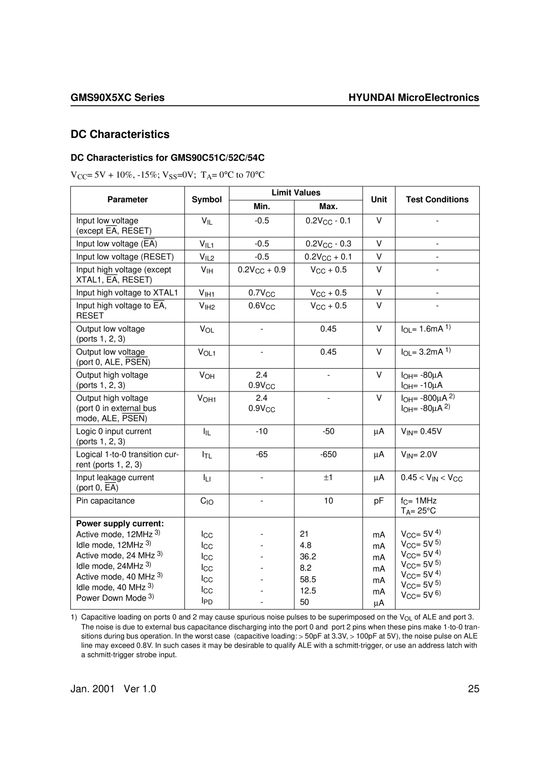
DC Characteristics
DC Characteristics for GMS90C51C/52C/54C
VCC= 5V + 10%, -15%; VSS=0V; TA= 0°C to 70°C
Parameter | Symbol |
| Limit Values | Unit | Test Conditions | ||||||
|
|
| |||||||||
| Min. | Max. | |||||||||
|
|
|
|
|
|
|
|
|
| ||
|
|
|
|
|
|
|
|
|
| ||
Input low voltage |
|
|
|
| VIL | 0.2VCC - 0.1 | V | - | |||
(except EA, RESET) |
|
|
|
|
|
| |||||
|
|
|
|
|
|
|
|
| |||
Input low voltage |
|
|
|
|
| VIL1 | 0.2VCC - 0.3 | V | - | ||
(EA) |
|
| |||||||||
Input low voltage (RESET) | VIL2 | 0.2VCC + 0.1 | V | - | |||||||
Input high voltage (except | VIH | 0.2VCC + 0.9 | VCC + 0.5 | V | - | ||||||
XTAL1, EA, RESET) |
|
|
|
|
|
| |||||
|
|
|
|
|
| ||||||
Input high voltage to XTAL1 | VIH1 | 0.7VCC | VCC + 0.5 | V | - | ||||||
Input high voltage to |
|
|
| VIH2 | 0.6VCC | VCC + 0.5 | V | - | |||
EA, |
| ||||||||||
RESET |
|
|
|
|
|
|
|
|
|
| |
|
|
|
|
|
|
|
|
|
| ||
Output low voltage |
|
|
|
| VOL | - | 0.45 | V | IOL= 1.6mA 1) | ||
(ports 1, 2, 3) |
|
|
|
|
|
|
|
|
|
| |
|
|
|
|
|
|
|
|
|
| ||
Output low voltage |
|
|
|
| VOL1 | - | 0.45 | V | IOL= 3.2mA 1) | ||
(port 0, ALE, PSEN) |
|
|
|
|
|
| |||||
|
|
|
|
|
| ||||||
Output high voltage | VOH | 2.4 | - | V | IOH= | ||||||
(ports 1, 2, 3) |
|
|
|
|
|
| 0.9VCC |
|
| IOH= | |
Output high voltage | VOH1 | 2.4 | - | V | IOH= | ||||||
(port 0 in external bus |
|
| 0.9VCC |
|
| IOH= | |||||
mode, ALE, PSEN) |
|
|
|
|
|
| |||||
|
|
|
|
|
| ||||||
Logic 0 input current | IIL | μA | VIN= 0.45V | ||||||||
(ports 1, 2, 3) |
|
|
|
|
|
|
|
|
|
| |
|
|
|
|
|
| ||||||
Logical | ITL | μA | VIN= 2.0V | ||||||||
rent (ports 1, 2, 3) |
|
|
|
|
|
|
|
|
|
| |
|
|
|
|
|
| ||||||
Input leakage current | ILI | - | ±1 | μA | 0.45 < VIN < VCC | ||||||
(port 0, EA) |
|
|
|
|
|
|
|
|
|
| |
|
|
|
|
|
|
|
|
|
| ||
Pin capacitance |
|
|
|
| CIO | - | 10 | pF | fC= 1MHz | ||
|
|
|
|
|
|
|
|
|
|
| TA= 25°C |
Power supply current: |
|
|
|
|
| VCC= 5V 4) | |||||
Active mode, 12MHz 3) | ICC | - | 21 | mA | |||||||
Idle mode, 12MHz | 3) |
|
|
| ICC | - | 4.8 | mA | V = 5V 5) | ||
|
|
|
| CC | |||||||
Active mode, 24 MHz 3) | ICC | - | 36.2 | mA | VCC= 5V 4) | ||||||
Idle mode, 24MHz 3) | ICC | - | 8.2 | mA | VCC= 5V 5) | ||||||
Active mode, 40 MHz 3) | ICC | - | 58.5 | mA | VCC= 5V 4) | ||||||
|
|
|
|
|
| 5) | |||||
Idle mode, 40 MHz 3) | ICC | - | 12.5 | mA | VCC= 5V 6) | ||||||
Power Down Mode 3) | IPD | - | 50 | μ | VCC= 5V | ||||||
|
|
|
|
|
|
|
| A |
| ||
1)Capacitive loading on ports 0 and 2 may cause spurious noise pulses to be superimposed on the VOL of ALE and port 3.
The noise is due to external bus capacitance discharging into the port 0 and port 2 pins when these pins make
line may exceed 0.8V. In such cases it may be desirable to qualify ALE with a
Jan. 2001 Ver 1.0 | 25 |