|
|
|
|
|
|
|
|
|
|
|
|
|
|
|
|
|
|
|
|
|
|
|
| CY7C024AV/024BV/025AV/026AV | ||
|
|
|
|
|
|
|
|
|
|
|
|
|
|
|
|
|
|
|
|
|
|
|
| CY7C0241AV/0251AV/036AV | ||
|
|
|
|
|
|
|
|
|
|
|
|
|
|
|
|
|
|
|
|
|
|
|
|
|
|
|
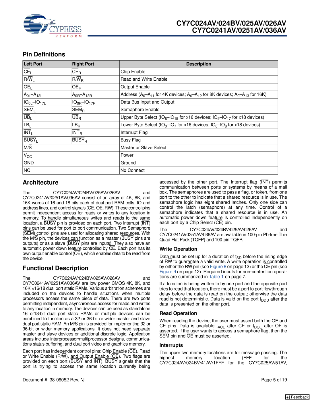
Pin Definitions |
|
|
|
|
|
|
|
|
|
|
|
|
|
| ||||||||||||
|
|
|
|
|
|
|
|
|
|
|
|
|
|
|
|
|
|
|
|
|
|
|
| |||
| Left Port |
| Right Port | Description |
|
| ||||||||||||||||||||
|
|
|
|
| L |
|
|
|
| R | Chip Enable |
| ||||||||||||||
| CE | CE | ||||||||||||||||||||||||
|
|
|
|
|
|
|
|
| L |
|
|
|
|
|
|
| R | Read and Write Enable |
| |||||||
| R/W | R/W | ||||||||||||||||||||||||
|
|
|
|
|
| L |
|
|
|
|
| R | Output Enable |
| ||||||||||||
| OE | OE | ||||||||||||||||||||||||
|
| Address |
|
| ||||||||||||||||||||||
|
| Data Bus Input and Output |
|
| ||||||||||||||||||||||
|
|
|
|
|
|
|
|
|
| L |
|
|
|
|
|
|
|
| R | Semaphore Enable |
| |||||
| SEM | SEM | ||||||||||||||||||||||||
|
|
|
|
| L |
|
|
|
| R | Upper Byte Select |
| ||||||||||||||
| UB | UB | ||||||||||||||||||||||||
|
|
|
| L |
|
|
| R | Lower Byte Select |
| ||||||||||||||||
| LB | LB | ||||||||||||||||||||||||
|
|
|
|
|
|
| L |
|
|
|
|
|
| R | Interrupt Flag |
| ||||||||||
| INT | INT | ||||||||||||||||||||||||
|
|
|
|
|
|
|
|
|
|
| L |
|
|
|
|
|
|
|
|
| R | Busy Flag |
| |||
| BUSY | BUSY | ||||||||||||||||||||||||
|
|
|
|
|
|
|
|
|
|
|
|
|
|
|
|
|
|
|
|
| Master or Slave Select |
| ||||
| M/S |
|
|
|
|
|
|
|
|
|
|
| ||||||||||||||
| VCC |
|
|
|
|
|
|
|
|
|
|
| Power |
|
| |||||||||||
| GND |
|
|
|
|
|
|
|
|
|
|
| Ground |
|
| |||||||||||
|
|
|
|
|
|
|
|
|
|
|
|
|
|
| ||||||||||||
| NC |
|
|
|
|
|
|
|
|
|
|
| No Connect |
|
| |||||||||||
|
|
|
|
|
|
|
|
|
|
|
|
|
|
|
|
|
|
|
|
|
|
|
|
|
|
|
Architecture
The CY7C024AV/024BV/025AV/026AV and CY7C0241AV/0251AV/036AV consist of an array of 4K, 8K, and 16K words of 16 and 18 bits each of
Functional Description
The CY7C024AV/024BV/025AV/026AV and CY7C0241AV/0251AV/036AV are low power CMOS 4K, 8K, and 16K ×16/18 dual port static RAMs. Various arbitration schemes are included on the devices to handle situations when multiple processors access the same piece of data. There are two ports permitting independent, asynchronous access for reads and writes to any location in memory. The devices can be used as standalone 16
Each port has independent control pins: Chip Enable (CE), Read or Write Enable (R/W), and Output Enable (OE). Two flags are provided on each port (BUSY and INT). BUSY signals that the port is trying to access the same location currently being
accessed by the other port. The Interrupt flag (INT) permits communication between ports or systems by means of a mail box. The semaphores are used to pass a flag, or token, from one port to the other to indicate that a shared resource is in use. The semaphore logic has eight shared latches. Only one side can control the latch (semaphore) at any time. Control of a semaphore indicates that a shared resource is in use. An automatic power down feature is controlled independently on each port by a Chip Select (CE) pin.
The CY7C024AV/024BV/025AV/026AV and CY7C0241AV0251AV/036AV are available in
Write Operation
Data must be set up for a duration of tSD before the rising edge of RW to guarantee a valid write. A write operation is controlled by either the RW pin (see Figure 8 on page 12) or the CE pin (see Figure 9 on page 12). Required inputs for
If a location is being written to by one port and the opposite port tries to read that location, there must be a port to port flowthrough delay before the data is read on the output; otherwise the data read is not deterministic. Data is valid on the port tDDD after the data is presented on the other port.
Read Operation
When reading the device, the user must assert both the OE and CE pins. Data is available tACE after CE or tDOE after OE is asserted. If the user wants to access a semaphore flag, then the SEM pin and OE must be asserted.
Interrupts
The upper two memory locations are for message passing. The
highest memory location (FFF for the CY7C024AV/024BV/41AV/1FFF for the CY7C025AV/51AV,
Document #: | Page 5 of 19 |
[+] Feedback