CY7C1218H specifications
The Cypress CY7C1218H is a high-performance synchronous static random-access memory (SRAM) device designed to meet the demanding requirements of advanced memory applications. This SRAM boasts a density of 2 Mbits, making it suitable for a variety of uses, including telecommunications, industrial, and consumer electronics.One of the main features of the CY7C1218H is its fast access time, which ranges from 10 ns to 15 ns, depending on the specific configuration. This high-speed access allows for efficient read/write operations and ensures that the memory can keep pace with the needs of high-speed processors and data buses. The device operates with a single 3.3V supply, enhancing its compatibility with modern digital circuits and reducing power consumption.
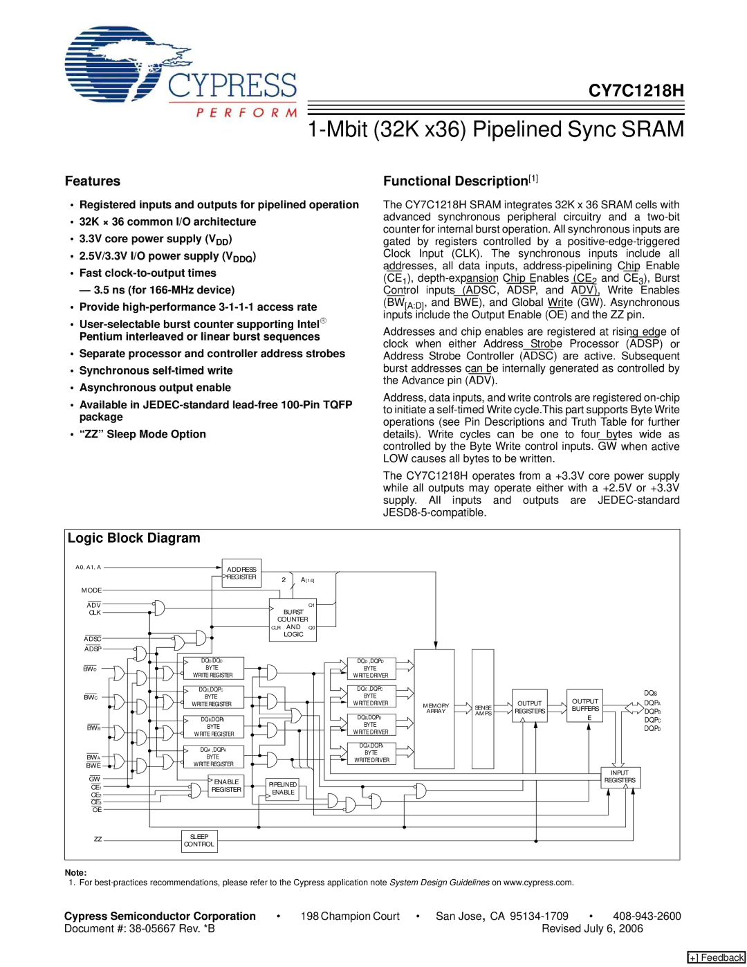
The CY7C1218H employs a synchronous interface that simplifies the control signaling process and increases data transfer rates. This synchronous nature means that the operation of the chip is synchronized with an external clock, facilitating faster and more reliable data transfer between the memory and the host system. This is particularly beneficial in high-performance applications where latency and throughput are critical.
In addition to its speed and efficiency, the CY7C1218H features a low standby power mode. This is an essential characteristic for battery-powered and energy-efficient systems, as it significantly reduces power consumption when the device is not actively in use. The SRAM design also includes a write protect feature, enhancing data integrity and security in sensitive applications.
The device is packaged in a 44-pin TSOP (Thin Small Outline Package) and has a compact footprint, making it suitable for space-constrained designs. The CY7C1218H uses advanced CMOS technology to support reliable performance and long data retention, ensuring that stored data remains intact even during power-down cycles.
Overall, the Cypress CY7C1218H represents a robust solution for engineers looking to integrate high-speed, low-power SRAM into their designs. Its blend of speed, reliability, and efficiency makes it an excellent choice for applications requiring fast access and secure data storage, making it a staple in various electronic systems across different industries.